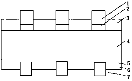
Homogenous crystal silicon double-sided solar cell structure with light incidence areas which are not covered by heavy doping layers
A double-sided solar cell, heavy doping technology, applied in the field of solar cells, can solve problems such as increased recombination rate, increased carrier recombination, and reduced lateral transmission loss, achieving high open circuit voltage and short circuit current, improving short circuit current, Improve the effect of built-in potential
- Summary
- Abstract
- Description
- Claims
- Application Information
AI Technical Summary
Problems solved by technology
Method used
Image
Examples
Embodiment 1
[0017] as attached figure 1 A homogeneous crystalline silicon double-sided solar cell structure is shown in which the light-incoming region is not shielded by a heavily doped layer. Both sides of the n-type crystalline silicon wafer 4 are all made of pyramid structure suede with an average of ~2 microns, the passivation anti-reflection layer I 3 and the passivation anti-reflection layer II 6 are all made of silicon nitride film, the metal grid line I 1 and the metal The grid lines II and 7 all adopt the Ag grid line structure with the main and auxiliary grids, and the covering area is 3% of the surface area of the silicon wafer. The structure has excellent double-sided light-incoming characteristics, that is, any side can be used as the main light-incoming surface. If it is used as a single-side light-incoming solar cell, a layer of metal can be plated on the backlight as a reflective layer to increase the short-circuit current of the single-side light-incoming solar cell. ...
Embodiment 2
[0020] as attached figure 1 A homogeneous crystalline silicon double-sided solar cell structure is shown in which the light-incoming region is not shielded by a heavily doped layer. The passivation-light-incoming regions on both sides of the n-type crystalline silicon wafer 4 adopt a pyramid structure suede surface with an average of ~1 micron, and the emitter-conducting region and the back electric field-conducting region adopt a chemically polished structure. The passivation anti-reflection layer I 3 adopts a silicon dioxide / silicon nitride composite thin film, and the passivation anti-reflection layer II 6 adopts a silicon nitride thin film. Both the metal grid line I 1 and the metal grid line II 7 adopt a Ni / Cu / Ag composite grid line structure with main and auxiliary grids, and the covering area is 1% of the surface area of the silicon wafer. The structure has excellent double-sided light-incoming characteristics, that is, any side can be used as the main light-incoming...
PUM
 Abstract
Description
Claims
Application Information
 - R&D
- Intellectual Property
- Life Sciences
- Materials
- Tech Scout
- Unparalleled Data Quality
- Higher Quality Content
- 60% Fewer Hallucinations
Browse by: Latest US Patents, China's latest patents, Technical Efficacy Thesaurus, Application Domain, Technology Topic, Popular Technical Reports.
© 2025 PatSnap. All rights reserved.Legal|Privacy policy|Modern Slavery Act Transparency Statement|Sitemap|About US| Contact US: help@patsnap.com

