Schottky solar cell and production method thereof
A technology for solar cells and back electrodes, applied in circuits, photovoltaic power generation, electrical components, etc., can solve the problems of complicated process, high manufacturing cost of silicon-based cells, high processing temperature, etc. Potential, the effect of increasing the short-circuit current
- Summary
- Abstract
- Description
- Claims
- Application Information
AI Technical Summary
Problems solved by technology
Method used
Image
Examples
preparation example Construction
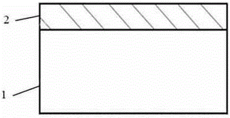
[0029] A method for preparing a Schottky solar cell, comprising the steps of:
[0030] a: Prepare a semiconductor layer, that is, cover the semiconductor on the substrate, then use a mixed solution of acetone and alcohol to sonicate in the ultrasonic wave for 20-35 minutes, then repeatedly rinse with deionized water several times to wash off the acetone and alcohol, and dry it with nitrogen for backup use;
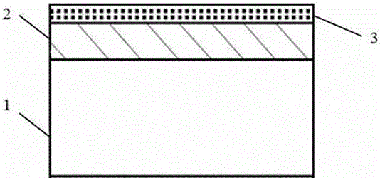
[0031] b: a magnetron sputtering system is used on the front side of the above-mentioned dried semiconductor layer, the target material is high-purity graphite and copper, the sputtering gas is argon, and sputtering has insulation and high light transmittance on the semiconductor layer. Carbon film, and then prepare copper film by in-situ sputtering on the carbon film; then anneal heat treatment by CVD technology, and catalyze the formation of single-layer or multi-layer graphene between the copper film and the carbon film in contact with the copper film, which is graphene...
Embodiment 1
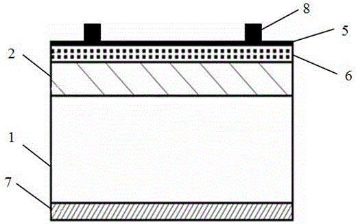
[0040] As shown in the figure: a Schottky solar cell that is a graphene / amorphous carbon / silicon dioxide Schottky solar cell, including an aluminum metal with a thickness of 300-3000nm as the back electrode, and a conductive silver with a thickness of 300-3000nm The glue is the positive electrode grid line and the semiconductor layer. The semiconductor layer is prepared by covering the silicon dioxide film 2 on the N-type single crystal silicon substrate 1, and its thickness is 10-300μm; it also includes amorphous carbon film I and graphene layer, the amorphous carbon film I is located between the semiconductor layer and the graphene layer; the front of the semiconductor layer is the amorphous carbon film I, and its thickness is 1.7-59.7nm; the back is the back electrode, and the window on the front of the graphene layer is surrounded by positive electrode grid line; the graphene layer is the anode, and its thickness is 0.3nm. Described graphene / amorphous carbon / silicon dioxid...
Embodiment 2
[0046] A Schottky solar cell is a graphene / amorphous carbon / silicon dioxide Schottky solar cell, comprising an aluminum metal with a thickness of 300-3000nm, i.e. a back electrode, and a conductive silver glue with a thickness of 300-3000nm, i.e. a positive electrode grid Wire and semiconductor layer, the semiconductor layer is prepared by covering a silicon dioxide film on an N-type single crystal silicon substrate, and its thickness is 10-300µm; it also includes an amorphous carbon film Ⅰ and a graphene layer, an amorphous carbon film Ⅰ It is located between the semiconductor layer and the graphene layer; the front side of the semiconductor layer is an amorphous carbon film I with a thickness of 1.4-59.7nm; the back side is the back electrode, and there are positive electrode grid lines around the window on the front side of the graphene layer; the graphene layer is the anode , its thickness is 0.3-0.6nm;.
[0047] The above-mentioned graphene / amorphous carbon / silicon dioxid...
PUM
| Property | Measurement | Unit |
|---|---|---|
| thickness | aaaaa | aaaaa |
| thickness | aaaaa | aaaaa |
| thickness | aaaaa | aaaaa |
Abstract
Description
Claims
Application Information
 - R&D
- Intellectual Property
- Life Sciences
- Materials
- Tech Scout
- Unparalleled Data Quality
- Higher Quality Content
- 60% Fewer Hallucinations
Browse by: Latest US Patents, China's latest patents, Technical Efficacy Thesaurus, Application Domain, Technology Topic, Popular Technical Reports.
© 2025 PatSnap. All rights reserved.Legal|Privacy policy|Modern Slavery Act Transparency Statement|Sitemap|About US| Contact US: help@patsnap.com


