


Quick Research
Generate reliable direction feasibility study reports for your R&D in just a few steps.

Technical Q&A
Discover and master advanced knowledge NOW. Basics, ideas, possibilities, all at once.

Find Solutions
As an expert in R&D theories, this can generate solutions to your technical problems instantly.

Evaluate Feasibility
Analyze your overall solution with one click, know your potential R&D risks in advance.

Monitor Landscape
Get weekly tech updates, stay abreast of the latest tech innovations and key insights.
Niobium telluride two-dimensional material as well as synthesis and application thereof
A technology of two-dimensional materials and raw materials, applied in the field of nanomaterials
- Summary
- Abstract
- Description
- Claims
- Application Information
AI Technical Summary
Problems solved by technology
Method used
Image

Examples
Embodiment 1
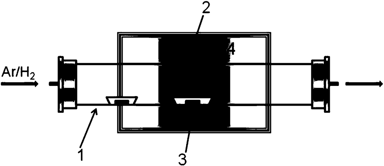
[0110] NbTe 2 Preparation of nanosheets:
[0111] Put the porcelain boat filled with 0.02g Te powder in high temperature constant temperature zone 2, filled with 0.1g NbCl 5 The porcelain boat of the powder is placed upstream of the Te powder, and the NbCl 5 The heating volatilization temperature of the powder is 200°C; a piece of Si / 285nm SiO 2 as NbTe 2 The bright side of the growth substrate was covered directly above the ceramic boat loaded with Te powder to obtain a suitable crystal growth temperature. Before heating, exhaust the air in the quartz tube with a large flow of argon. Then heat the constant temperature zone 2 to 550°C (the heating volatilization temperature of Te powder is 550°C; the deposition temperature is 550°C), and set the carrier gas flow rate to 80 / 8sccm (Ar / H 2 ), constant temperature for 10min, there will be ultra-thin single crystal NbTe on the silicon wafer 2 Nanosheet generation. NbTe 2 The experimental setup of the nanosheets is shown in ...
Embodiment 2
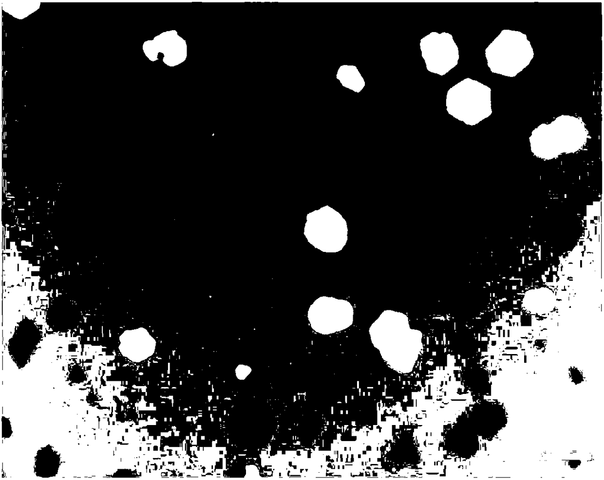
[0115] Compared with Example 1, the difference is that the substrate temperature is 550° C., the flow rate is 200 / 20 sccm, and the deposition time is 10 min. Figure 4 For the prepared NbTe 2 Optical schematic diagram of nanosheet, Si / SiO 2 The base is light purple, and the white, light purple, and dark purple hexagons / triangles represent different thicknesses of NbTe 2 (from thick to thin), compared with embodiment 1, increased carrier gas flow, the NbTe obtained under this condition 2 The nanosheets are larger in size and have good crystallinity, the thickness can be as thin as 4.5nm, and the thickness is less than 300nm, and the size is 3-15μm. Figure 4 The scale bar in is 10 μm.
Embodiment 3
[0117] Compared with Example 1, the difference is that the substrate temperature is 550° C., the flow rate is 30 / 3 sccm, and the deposition time is 10 min. Figure 5 For the prepared NbTe 2 Optical schematic diagram of nanosheet, Si / SiO 2 The base is light red, and the white, light purple, dark purple hexagons / triangles represent different thicknesses of NbTe 2 (From thick to thin); Compared with Example 1, the carrier gas flow rate is reduced, and the obtained NbTe2 overall thickness becomes thicker and the size becomes smaller. Among them, the thinnest thickness is 8nm, the thickest is 380nm, and the size is 2-5μm. Figure 5 The scale bar in is 10 μm. Non-preferred flow, the obtained effect is slightly worse than that of Example 1, for example, the thickness of the obtained two-dimensional material will be slightly thicker.
PUM
| Property | Measurement | Unit |
|---|---|---|
| thickness | aaaaa | aaaaa |
| thickness | aaaaa | aaaaa |
| thickness | aaaaa | aaaaa |
Abstract
Description
Claims
Application Information
 - R&D Engineer
- R&D Manager
- IP Professional
- Industry Leading Data Capabilities
- Powerful AI technology
- Patent DNA Extraction
Browse by: Latest US Patents, China's latest patents, Technical Efficacy Thesaurus, Application Domain, Technology Topic, Popular Technical Reports.
© 2024 PatSnap. All rights reserved.Legal|Privacy policy|Modern Slavery Act Transparency Statement|Sitemap|About US| Contact US: help@patsnap.com