Unlock instant, AI-driven research and patent intelligence for your innovation.

Semiconductor wafer etching method

A semiconductor and wafer technology, applied in the field of semiconductor wafer etching, can solve the problems of insufficient plasma bombardment on the wafer, the etching efficiency of the semiconductor wafer needs to be improved, and the etching efficiency of the bottom of the semiconductor wafer is low. The effect of improving the etching effect, increasing the speed, and increasing the efficiency

Active Publication Date: 2018-09-04
浙江蓝晶芯微电子有限公司
View PDF6 Cites 2 Cited by
  • Summary
  • Abstract
  • Description
  • Claims
  • Application Information

AI Technical Summary

Problems solved by technology

"Although this technical solution can also improve the efficiency of wafer etching, the bombardment of the generated plasma on the wafer is not strong enough to effectively remove the waste generated when the plasma bombards the wafer, so that most of the plasma bombards the wafer surface The bombardment force cannot be effectively utilized; when the thickness of the semiconductor wafer is large, the etching efficiency at the bottom of the semiconductor wafer is low, and the etching efficiency of the semiconductor wafer needs to be improved

Method used


Image

  • Semiconductor wafer etching method
  • Semiconductor wafer etching method
  • Semiconductor wafer etching method

Examples


specific Embodiment 1

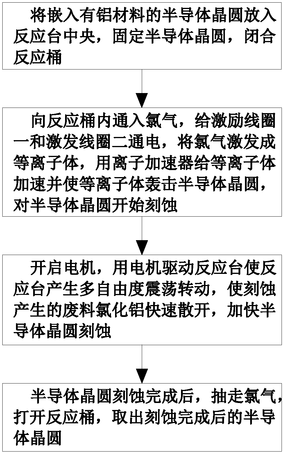
[0044] Specific embodiment one: fix the semiconductor wafer 9 by the reaction table 5, after closing the reaction barrel 1; feed chlorine gas into the reaction barrel 1 with the gas inlet pipe 11, and the gas heating pipeline 13 will continuously remove the gas in the reaction barrel 1 Heating, the temperature in the reaction barrel 1 is raised, and the temperature of the aluminum material 91 on the semiconductor wafer 9 is raised. At the same time, the excitation coil one 2 and the excitation coil two 41 are energized, and the excitation coil one 2 will energize the outside of the fixed sleeve 4. The chlorine gas is excited into plasma, and the electric field generated by the excitation coil one 2 makes the plasma continuously bombard the semiconductor wafer 9, and the excitation coil two 41 excites the chlorine gas in the fixed sleeve 4 into plasma, and the plasma enters the ion accelerator 3; the ion accelerator 3 is turned on , the ion accelerator 3 accelerates the plasma a...

specific Embodiment 2

[0046] Specific embodiment two: fix the semiconductor wafer 9 by the reaction table 5, after closing the reaction barrel 1; feed chlorine gas into the reaction barrel 1 with the gas inlet pipe 11, and the gas heating pipeline 13 will continuously remove the gas in the reaction barrel 1 Heating, the temperature in the reaction barrel 1 is raised, the temperature of the aluminum material 91 on the semiconductor wafer 9 is raised, and at the same time, the excitation coil one 2 and the excitation coil two 41 are energized, and the excitation coil one 2 will energize the outside of the fixed sleeve 4. The chlorine gas is excited into plasma, the electric field generated by the excitation coil 1 2 makes the plasma continuously bombard the semiconductor wafer 9, the excitation coil 2 41 excites the chlorine gas in the fixed sleeve 4 into plasma, the plasma enters the ion accelerator 3, and the ion accelerator 3 is turned on , the ion accelerator 3 accelerates the plasma and makes the...


PUM


Abstract

The invention belongs to the semiconductor technology field and especially relates to a semiconductor wafer etching method. In the etching method, a semiconductor wafer etching device is adopted. Thesemiconductor wafer etching device comprises a reaction barrel, an excitation coil 1, an ion accelerator, a fixing sleeve, a reaction stage, an oscillating unit and a motor. The excitation coil 1 sleeves the reaction barrel. The excitation coil 1 is used to excite an etching gas in the reaction barrel into a plasma. The fixing sleeve is fixed to the lower end of a gas introduction pipe. The ion accelerator is used for accelerating the plasma so as to bombard a semiconductor wafer. The reaction stage is located right below the ion accelerator. The motor drives the oscillating unit to rotate. The oscillating unit drives the reaction stage to generate multiple-freedom-degree oscillating rotation so as to realize automatic disengagement of etched waste aluminum chloride on a semiconductor wafer. In the invention, an etched waste is timely and effectively eliminated so that the etching efficiency and the etching effect of the semiconductor wafer are increased.

Description

technical field [0001] The invention belongs to the technical field of semiconductor technology, in particular to a semiconductor wafer etching method. Background technique [0002] Wafer refers to the silicon wafer used in the production of silicon semiconductor integrated circuits. Because of its circular shape, it is called a wafer. It can be processed into various circuit element structures on the silicon wafer and become a product with specific electrical functions. . The raw material of the wafer is silicon, and the surface of the earth's crust has an inexhaustible amount of silicon dioxide. Silicon dioxide ore is refined by electric arc furnace, chlorinated with hydrochloric acid, and distilled to produce high-purity polysilicon. The wafer manufacturing plant melts the polysilicon, and then plants seed crystals in the melt, and then slows it down. Slowly pulled out to form a cylindrical single crystal silicon ingot. Since the silicon ingot is gradually formed from a...

Claims


Application Information

Patent Timeline
IPC IPC(8): H01L21/3213H01J37/32
CPCH01J37/32137H01J37/32449H01J2237/3348H01L21/32136
Inventor 梁亚梁志强
Owner 浙江蓝晶芯微电子有限公司