Fabrication method of ultra-thin silicon transfer plate without temporary bonding and un-bonding processes

A production method and temporary bonding technology, which is applied in semiconductor/solid-state device manufacturing, electrical components, circuits, etc., can solve the problems of colloid residual pollution, high equipment cost, and many process steps, and achieve low process cost and high reliability , The effect of low process difficulty

Active Publication Date: 2018-09-07
CHINA ELECTRONIC TECH GRP CORP NO 38 RES INST
View PDF9 Cites 8 Cited by
  • Summary
  • Abstract
  • Description
  • Claims
  • Application Information

AI Technical Summary

Problems solved by technology

[0005] In view of the above-mentioned shortcomings of the prior art, the purpose of the present invention is to provide a method for manufacturing an ultra-thin silicon adapter plate without temporary bonding and debonding processes, which is used to solve the problems of high equipment cost, many process steps, and colloidal The problem of residual contamination

Method used


Image

  • Fabrication method of ultra-thin silicon transfer plate without temporary bonding and un-bonding processes
  • Fabrication method of ultra-thin silicon transfer plate without temporary bonding and un-bonding processes
  • Fabrication method of ultra-thin silicon transfer plate without temporary bonding and un-bonding processes

Examples


Embodiment 1

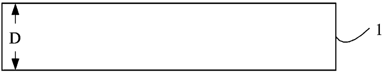
[0047] A method for making an ultra-thin silicon adapter plate without temporary bonding, which is suitable for making an ultra-thin silicon adapter plate. The thickness range of the obtained ultra-thin silicon adapter plate is between 50-200 μm, and the area is 25mm×25mm , the wiring width is more than 1 μm, and the through-silicon via has a diameter of more than 30 μm, and the said through-silicon via is only used for side wall metallization and has no solid hole feature.

[0048] As a specific embodiment, in this embodiment, an ultra-thin silicon interposer board with a thickness of 150 μm, an area of ​​25 mm×25 mm, a wiring width of 20 μm, and a TSV diameter of 60 μm is taken as an example for illustration.

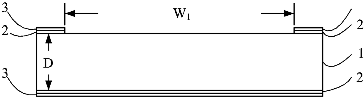
[0049] In this embodiment, the side of the ultra-thin silicon interposer silicon chip where the chip circuit is arranged is called the front side, and the other side opposite to the chip circuit is called the back side.

[0050] The manufacturing method of the ultra-t...

Embodiment 2

[0074] The difference between this embodiment and embodiment 1 is that the process methods of step 3 and step 10 are adjusted, and other steps are the same as embodiment 1. Compared with Embodiment 1, this embodiment is more suitable for making an ultra-thin silicon interposer with a thickness less than 100 μm.

[0075] As a specific embodiment, in this embodiment, an ultra-thin silicon interposer board with a thickness of 50 μm, an area of ​​25 mm×25 mm, a wiring line width of 20 μm, and a TSV diameter of 60 μm is taken as an example for illustration.

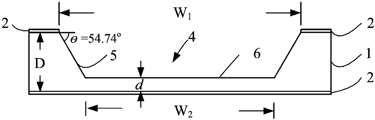
[0076] In step 3 of this embodiment, a silicon cavity 4 with a depth of 180 μm is manufactured, that is, the thickness d of the functional region of the interposer board obtained is 100 μm.

[0077] Step 10 of this embodiment specifically includes:

[0078] On the front side of the silicon wafer 1, spray glue to form a photoresist protective layer; on the back side of the silicon wafer 1, remove the silicon dioxide layer on t...


PUM


Abstract

The invention provides a fabrication method of an ultra-thin silicon transfer plate without temporary bonding and un-bonding processes, and aims to solve the problems of high cost of equipment, largenumber of process steps and colloid residue pollution in the prior art. According to the fabrication method provided by the invention, the ultra-thin silicon transfer plate is formed in the silicon cavity of an ordinary silicon wafer, and holding and subsequent wiring layer processes and chip mounting can be operated like the ordinary silicon wafer, thus eliminating the expensive and complicated process steps of temporary bonding and un-bonding. The bottom plane of the silicon cavity fabricated by wet etching has a smooth surface, and does not need to carry out surface grinding and polishing process steps. In conjunction with glue spraying and laser direct writing lithography processes, the fabrication of a re-wiring layer can be completed, thus greatly lowering the process cost. A siliconthrough hole formed by laser processing has an inclined side wall, which is favorable for forming a high quality through hole barrier layer on the side wall of the silicon through hole and forming acomplete and continuous through hole side wall metal layer in the through hole.

Description

technical field [0001] The invention belongs to the technical field of three-dimensional high-density packaging and interconnection, and relates to a silicon transfer board structure and a wafer-level manufacturing method thereof. Background technique [0002] With the development of light weight, thinner, miniaturized, increasing number of I / O ports and diversified functions, traditional two-dimensional integration technology can no longer meet the requirements of high density, and problems such as signal distortion and delay are becoming more and more serious. System integration design Teachers began to turn more and more to three-dimensional integration (3DIntegration), system-level integration technology. [0003] Silicon is an ideal substrate material for wafer-level and three-dimensional integration. It has good mechanical and thermal properties and is an important semiconductor material. The processing technology of silicon materials is mature, and various micromachi...

Claims


Application Information

Patent Timeline
Patent Type & Authority Applications(China)
IPC IPC(8): H01L21/02H01L21/027
CPCH01L21/02104H01L21/02164H01L21/02175H01L21/027
Inventor 王强文郭育华王运龙刘建军宋夏邱颖霞
Owner CHINA ELECTRONIC TECH GRP CORP NO 38 RES INST
Why Eureka
Try Eureka