Optimized L-type tunneling field effect transistor and preparation method thereof

A tunneling field effect and transistor technology, applied in semiconductor/solid-state device manufacturing, diodes, semiconductor devices, etc., can solve the problems of serious bipolar effect, application limitation, small driving current, etc., to suppress bipolar effect, tunneling The effect of reduced probability and narrow forbidden band width

Active Publication Date: 2018-09-14
西安电子科技大学重庆集成电路创新研究院
View PDF2 Cites 7 Cited by
  • Summary
  • Abstract
  • Description
  • Claims
  • Application Information

AI Technical Summary

Problems solved by technology

However, compared with MOSFET devices, silicon-based TFET devices still face the problems of small driving current and serious bipolar effect, which limits their application.

Method used


Image

  • Optimized L-type tunneling field effect transistor and preparation method thereof
  • Optimized L-type tunneling field effect transistor and preparation method thereof
  • Optimized L-type tunneling field effect transistor and preparation method thereof

Examples


Embodiment 1

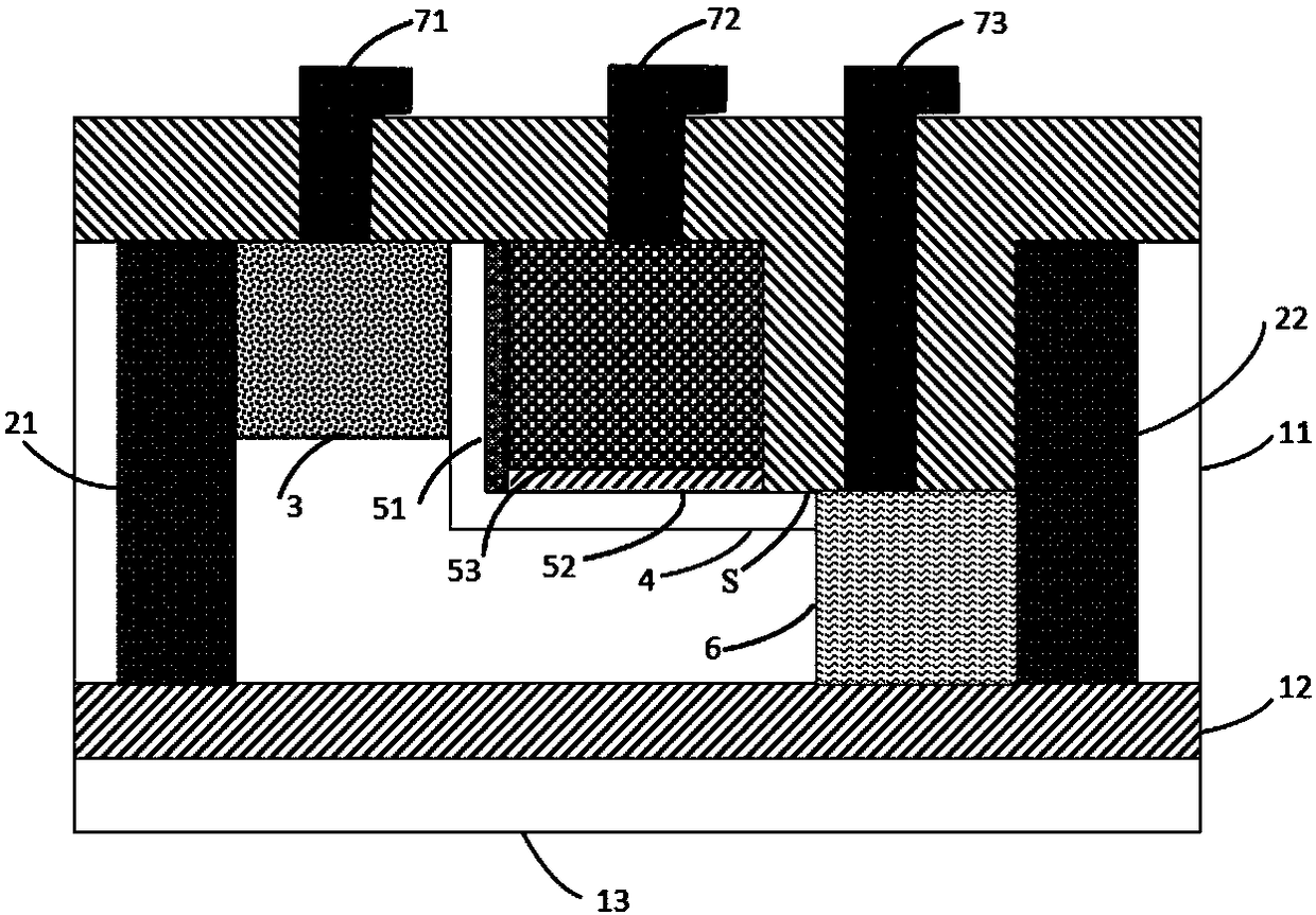
[0030] Embodiment 1, manufacturing a tunneling field effect transistor in which the distance between the drain region and the right border of the gate region is a quarter of the gate length.

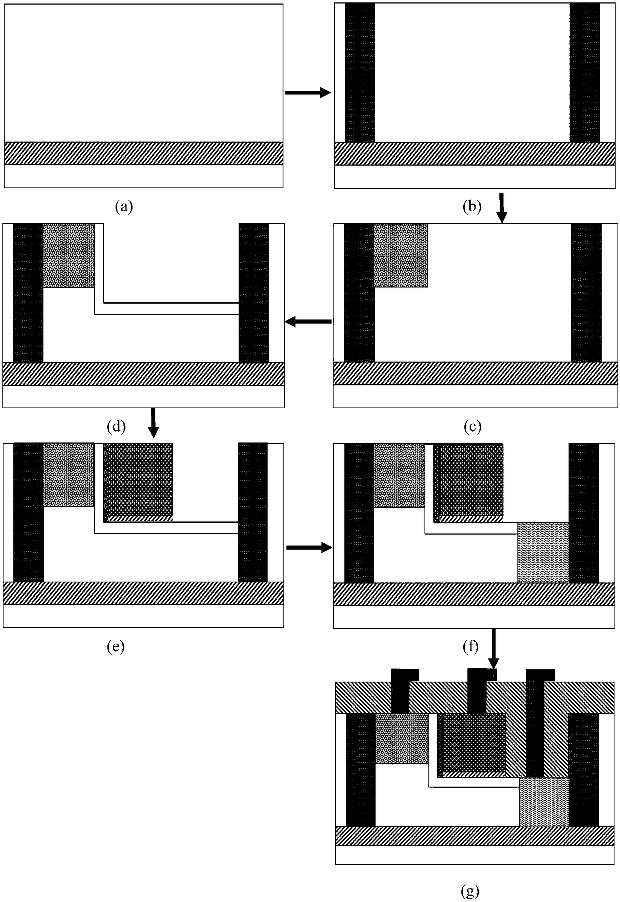
[0031] Step 1, make SOI substrate, such as figure 2 (a).

[0032] 1a) dry oxygen oxidation on the underlying initial silicon wafer to form a buried oxide layer;

[0033] 1b) A top silicon epitaxial layer is grown on the buried oxide layer by an epitaxial growth process to form an SOI substrate.

[0034] Step 2, etching on both sides of the top layer of silicon to form isolation grooves, such as figure 2 (b).

[0035] 2a) Growth of SiO on the top silicon surface of the SOI substrate 2 , forming the first SiO 2 layer, and then grow the first Si on the surface of the layer 3 N 4 layer, forming the first protective layer;

[0036] 2b) using a photolithography machine to form a shallow trench isolation pattern on the first protection layer by a photolithography process;

[0037] 2c...

Embodiment 2

[0067] Embodiment 2, manufacturing a tunneling field effect transistor in which the distance between the drain region and the right border of the gate region is half the gate length.

[0068] Step 1, making SOI substrate, such as figure 2 (a).

[0069] The specific implementation of this step is the same as Step 1 of Example 1.

[0070] Step 2, etching on both sides of the top layer of silicon to form isolation grooves, such as figure 2 (b).

[0071] The specific implementation of this step is the same as step 2 of embodiment 1.

[0072] Step 3, forming a doping concentration of 10 on the top silicon surface 19 cm -3 source area, such as figure 2 (c).

[0073] 3.1) Growth of SiO on top silicon surface 2 , forming a second SiO 2 layer, and then grow a second Si on the surface of the layer 3 N 4 layer, forming a second protective layer;

[0074] 3.2) using a photolithography machine to form a source region pattern at a set position on the second protective layer b...

Embodiment 3

[0089] Embodiment 3, manufacturing a tunneling field effect transistor in which the distance between the drain region and the right border of the gate region is three quarters of the gate length.

[0090] The first step is to make the SOI substrate, such as figure 2 (a).

[0091] The specific implementation of this step is the same as Step 1 of Example 1.

[0092] The second step is to etch and form isolation grooves on both sides of the top silicon, such as figure 2 (b).

[0093] The specific implementation of this step is the same as step 2 of embodiment 1.

[0094] The third step is to form a doping concentration of 10 on the top silicon surface 20 cm -3 source area, such as figure 2 (c).

[0095] First, grow SiO on the top silicon surface 2 , forming a second SiO 2 layer, and then grow a second Si on the surface of the layer 3 N 4 layer, forming a second protective layer;

[0096] Next, using a photolithography machine, a source region pattern is formed at a...


PUM


Abstract

The invention discloses an optimized L-type tunneling field effect transistor and a preparation method thereof and mainly solves the problems of low on state current and severe bipolar effect of an existing device. The optimized L-type tunneling field effect transistor comprises an SOI (silicon on insulator) substrate (1), isolation grooves (2), a source region (3), a channel region (4), a drain region (6), a gate region (5) and a conducting layer (7), wherein the isolation grooves (2) are located on two sides of the SOI substrate (1), and the source region (3), the channel region (4) and thedrain region (6) are located on the upper surface of the SOI substrate; the gate region (5) is located on the upper side of the channel region (4); the source region (3) is made of a germanium semiconductor material, the gate region (5) is of a hetero-gate dielectric structure, a high-k dielectric material is adopted on one side close to the source region, and a low-k dielectric material is adopted on one side close to the drain region; a space S is formed between the drain region (6) and the right margin of the gate region (5). The optimized L-type tunneling field effect transistor can effectively inhibit the bipolar effect, increases drive current and can be applied to manufacture of large-scale integrated circuits.

Description

technical field [0001] The invention belongs to the technical field of semiconductor devices, and in particular relates to an optimized L-type tunneling field effect transistor and a preparation method thereof, which can be used in the manufacture of large-scale integrated circuits. Background technique [0002] With the advancement of semiconductor integration technology, the development of integrated circuit technology following "Moore's law" has entered the nanometer scale. However, challenges from short-channel effects, parasitic effects, and quantum tunneling make it increasingly difficult to scale down conventional CMOS transistors, and it is difficult to meet the requirements of continuous development of integrated circuits. [0003] Tunneling Field Effect Transistor TFET works based on the quantum tunneling effect mechanism of band tunneling. At room temperature, the subthreshold swing can break through the limitation of the traditional MOSFET subthreshold limit valu...

Claims


Application Information

Patent Timeline
Patent Type & Authority Applications(China)
IPC IPC(8): H01L29/739H01L21/336H01L29/08
CPCH01L29/0843H01L29/66356H01L29/7391
Inventor 李聪闫志蕊庄奕琪赵小龙郭嘉敏
Owner 西安电子科技大学重庆集成电路创新研究院
Why Eureka
Try Eureka