Method for growing heterojunction in silicon microchannel plate

A technology of silicon microchannel plate and heterojunction, which is applied in the field of growing heterojunction, can solve the problems of complex process and high cost of molybdenum disulfide/graphene, and achieve the effects of low cost, environmental friendliness and overcoming complex process

Inactive Publication Date: 2018-09-28
CHANGSHU INSTITUTE OF TECHNOLOGY
View PDF6 Cites 4 Cited by
  • Summary
  • Abstract
  • Description
  • Claims
  • Application Information

AI Technical Summary

Problems solved by technology

[0007] Aiming at the above-mentioned deficiencies in the prior art, the present invention proposes a method for growing a heterojunction in a silicon microchannel plate, which overcomes the difficulty that molybdenum disulfide/graphene can be plugged into a nickel-plated silicon microchannel by electroplating technology ; At the same time

Method used


Image

  • Method for growing heterojunction in silicon microchannel plate
  • Method for growing heterojunction in silicon microchannel plate
  • Method for growing heterojunction in silicon microchannel plate

Examples


Embodiment 1

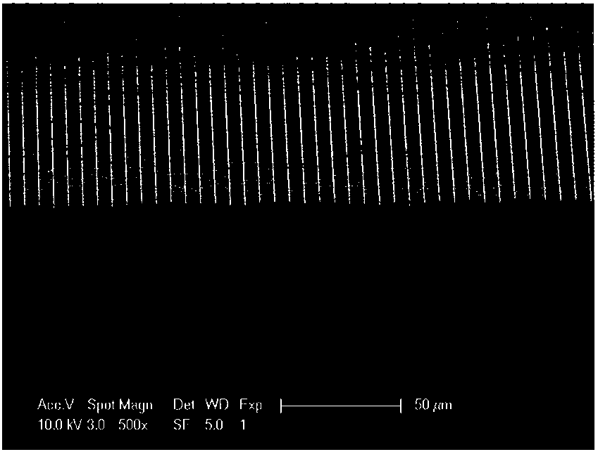
[0039] Such as figure 1 The silicon microchannel plate used in this embodiment shown is made of crystal-oriented P-type silicon, and its size is at the micron level, so it is also called macroporous silicon; the size of the silicon microchannel is 5×5×250 μm, the depth is The aspect ratio is 50.

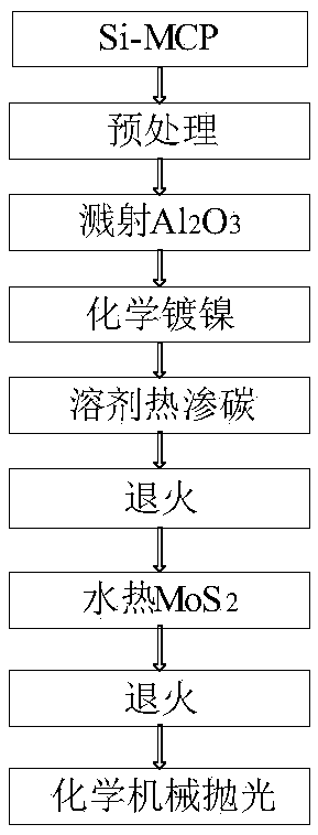
[0040] Such as figure 2 As shown, the specific process of heterojunction growth is as follows:

[0041] 1) Pretreatment;

[0042] Take 50ml of corrosion solution to soak the silicon microchannel plate, remove the silicon dioxide naturally grown on the surface of the silicon microchannel, blow dry with nitrogen, and dry it for later use; the composition of the corrosion solution includes HF, C 2 h 5 OH and H 2 O, the volume ratio of the three is 100:125:10, soak for 3 minutes;

[0043] 2) sputtering aluminum oxide;

[0044] Using the oblique sputtering method, select a sputtering angle of 30° to sputter aluminum oxide to the silicon microchannel to form a 5nm thick film;

[...

Embodiment 2

[0059] The specific process of heterojunction growth in this embodiment is as follows:

[0060] 1) Pretreatment;

[0061] Take 50ml of corrosion solution to soak the silicon microchannel plate, remove the silicon dioxide naturally grown on the surface of the silicon microchannel, blow dry with nitrogen, and dry it for later use; the composition of the corrosion solution includes HF, C 2 h 5 OH and H 2 O. The volume ratio of the three is 60:70:6, soak for 5 minutes;

[0062] 2) sputtering aluminum oxide;

[0063] Using the oblique sputtering method, select the sputtering angle of 40° to sputter aluminum oxide to the silicon microchannel to form a 10nm thick film;

[0064] 3) Electroless nickel plating;

[0065] First soak the silicon microchannel plate with Al2O3 in the surfactant to improve the wettability of the silicon microchannel and the surface of the silicon microchannel plate to activate the silicon and drive out the air in the silicon microchannel; the surfactant ...

Embodiment 3

[0078]The specific process of heterojunction growth in this embodiment is as follows:

[0079] 1) Pretreatment;

[0080] Take 50ml of corrosion solution to soak the silicon microchannel plate, remove the silicon dioxide naturally grown on the surface of the silicon microchannel, blow dry with nitrogen, and dry it for later use; the composition of the corrosion solution includes HF, C 2 h 5 OH and H 2 O. The volume ratio of the three is 80:100:9, soak for 3 minutes;

[0081] 2) sputtering silicon dioxide;

[0082] Using the oblique sputtering method, select a sputtering angle of 50° to sputter silicon dioxide to the silicon microchannel to form a 15nm thick film;

[0083] 3) Electroless nickel plating;

[0084] First soak the silicon microchannel plate with silicon dioxide in the surfactant to improve the wettability of the silicon microchannel and the surface of the silicon microchannel plate to activate the silicon and drive out the air in the silicon microchannel; the s...


PUM

PropertyMeasurementUnit
Thicknessaaaaaaaaaa

Abstract

The invention provides a method for growing a heterojunction in a silicon microchannel plate in the technical field of microelectromechnical systems. The method comprises the following steps: S1, immersing the silicon microchannel plate into a surfactant to eliminate air in a silicon microchannel and activate silicon, and then putting the silicon microchannel plate into a chemical nickel-plating solution to plate porous nickel; S2, putting a nickel plated silicon microchannel plate into a polyalcohol mixed with a sodium salt catalyst for ultrasonic processing and then performing a solvent thermal reaction to form a nickel plated silicon microchannel plate having an inner wall coated by a nickel carbide; S3, then annealing to obtain a nickel plated silicon microchannel plate having the inner wall coated by graphene; and S4, putting the nickel plated silicon microchannel plate having the inner wall coated by the graphene into a sulfur source and molybdenum source mixed solvent for a heating reaction to form a nickel plated silicon microchannel plate having the inner wall coated by a molybdenum disulfide/graphene heterojunction. According to the method provided by the invention, through chemical nickel plating, solvent thermal carburization and hydrothermal synthesis performed step by step, the heterojunction can be grown in the silicon microchannel; and the method is environment-friendly, simple to operate and low in cost.

Description

technical field [0001] The invention relates to a technology in the field of micro-electromechanical systems, in particular to a method for growing a heterojunction in a silicon micro-channel plate. Background technique [0002] Different two-dimensional materials constitute heterostructures that not only inherit the characteristics of high specific surface area of ​​two-dimensional materials, but also have unique physical and chemical properties. In recent years, the van der Waals heterostructure composed of graphene and two-dimensional sulfide has become a research hotspot for researchers. The main structures include lateral heterostructure and vertical heterostructure, which are widely used in supercapacitors, field-induced electrons Emission, Li-ion batteries, electrocatalysis and optoelectronic devices and other fields. However, the weak coupling and limited effective interface of the van der Waals heterostructure composed of graphene and two-dimensional sulfide inhibi...

Claims


Application Information

Patent Timeline
IPC IPC(8): B81C1/00
CPCB81C1/00349B81C2201/01
Inventor 吴大军陶石张磊高晓蕊
Owner CHANGSHU INSTITUTE OF TECHNOLOGY
Why Eureka
Try Eureka