Production method for MEMS air mass flow meter with back-cavity structure

A technology of air mass flow rate and manufacturing method, applied in the direction of microstructure technology, microstructure device, manufacturing microstructure device, etc., can solve the problem of affecting chip performance and yield, unstable resistance of thermistor, and poor adhesion of metal film and other problems, to achieve good line width control ability, stable resistance characteristics, and ensure the effect of adhesion

Inactive Publication Date: 2018-10-16
BEIJING INST OF AEROSPACE CONTROL DEVICES
View PDF9 Cites 6 Cited by
  • Summary
  • Abstract
  • Description
  • Claims
  • Application Information

AI Technical Summary

Problems solved by technology

[0005] The air quality and air flow sensitive chip is manufactured based on the combined micromachining process of the silicon substrate. In the actual processing process, due to the complex process parameters, there are excessive thermal stress, poor adhesion of the metal film, easy rupture of the suspended film, and low resistance of the thermistor. Stability and other issues have seriously affected the performance and yield of the chip

Method used


Image

  • Production method for MEMS air mass flow meter with back-cavity structure
  • Production method for MEMS air mass flow meter with back-cavity structure

Examples


Embodiment Construction

[0026] The present invention will be further described below in conjunction with the accompanying drawings.

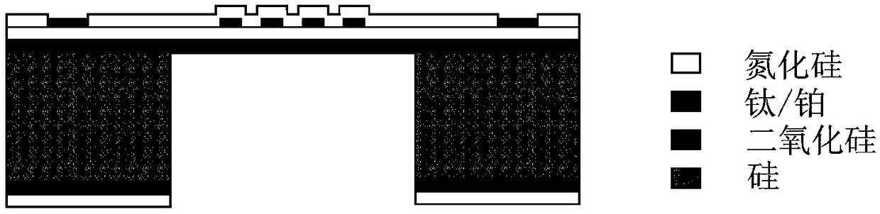
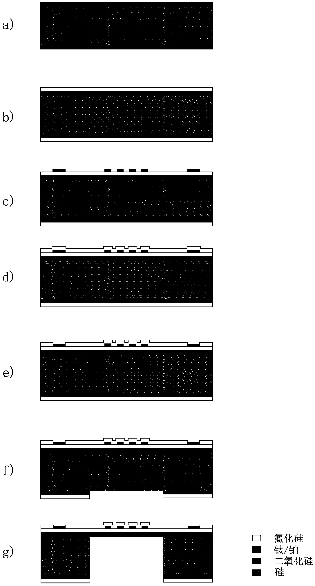
[0027] The method for manufacturing a chip of a silicon-based air mass flowmeter with a back cavity structure mainly includes the following steps: 1) forming a composite dielectric film on the surface of a silicon chip; 2) preparing a metal thermistor film pattern by a stripping method; A protective layer is grown on the surface of the metal thermistor film; 4) high-temperature annealing is performed; 5) the protective layer on the pad is removed by photoetching and corrosion, and the metal layer is exposed; 6) the back is photo-etched and dry-etched to form a back cavity structure; 7) Chip cutting into lobes to complete chip processing. The schematic diagram of the structure of the chip is as follows figure 1 shown.

[0028] Silicon wafers with a thickness of 200um-400um are selected for the processing of silicon-based air mass flowmeter chips, and the crystal orien...


PUM

PropertyMeasurementUnit
thicknessaaaaaaaaaa

Abstract

The invention relates to a production method for an MEMS air mass flow meter with a back cavity structure. The method comprises the steps of forming composite dielectric film on a surface of a siliconwafer; preparing a metal thermistor thin film pattern through utilization of an exfoliation method; growing a protection layer on the surface of metal thermistor thin film; carrying out high temperature annealing; removing the protection layer on a bonding pad and exposing a metal layer of the bonding pad; carrying out photoetching on the back of the silicon wafer, and carrying out dry etching, thereby forming the back cavity structure; and cutting and splitting chips, thereby finishing processing the chips. According to the method, after photoetching, development and plasma glue extrusion steps are carried out, a deionized water washing step is imported, so residual impurities on the surface of the wafer can be effectively removed after the plasma washing is carried out, the adhesion ofthe metal film on the dielectric film is ensured, and the metal film is prevented from falling off. According to the method, through utilization of a back dry etching technology, a back cavity is realized, and a corrosive effect of corrosive liquid in wet etching for a front pattern structure can be effectively prevented.

Description

technical field [0001] The invention belongs to the field of MEMS manufacturing, and relates to a method for manufacturing a MEMS air mass flowmeter chip with a back cavity structure, in particular to a method for manufacturing an air mass flow meter chip with a film back cavity. Background technique [0002] The air mass flow sensor for vehicle is an electronic device used in the electronic control system of modern vehicles. Installed between the air filter and the throttle valve, it is used to measure the amount of air inhaled into the engine, which is converted into an electrical signal and then transmitted to the ECU as a parameter to determine the basic fuel injection volume. The air flow sensor is used to measure the air intake volume. The sensor is one of the important components that determine the control accuracy of the system. [0003] The hot-film air mass flow sensor belongs to the calorimetric sensor. According to the theory proposed by Thomas that "the heat re...

Claims


Application Information

Patent Timeline
Patent Type & Authority Applications(China)
IPC IPC(8): B81B7/02B81C1/00
CPCB81B7/02B81B2201/0292B81C1/00015
Inventor 刘福民邱飞燕梁德春刘宇张树伟徐宇新
Owner BEIJING INST OF AEROSPACE CONTROL DEVICES
Why Eureka
Try Eureka