Manufacturing method for IGBT chip with composite grid

A fabrication method and compound gate technology, applied in the fields of semiconductor/solid-state device manufacturing, electrical components, semiconductor devices, etc., can solve problems such as the inability to improve the current density and withstand voltage capability of the chip, and achieve optimized current density distribution and thermal balance, and optimized electric field distribution. , Improve the effect of reverse bias resistance and high temperature capability

Active Publication Date: 2018-10-19
ZHUZHOU CRRC TIMES SEMICON CO LTD
View PDF3 Cites 10 Cited by
  • Summary
  • Abstract
  • Description
  • Claims
  • Application Information

AI Technical Summary

Problems solved by technology

[0005] The technical problem to be solved by the present invention is that the insulated gate bipolar transistor chip made by the prior...

Method used


Image

  • Manufacturing method for IGBT chip with composite grid
  • Manufacturing method for IGBT chip with composite grid
  • Manufacturing method for IGBT chip with composite grid

Examples


Embodiment 1

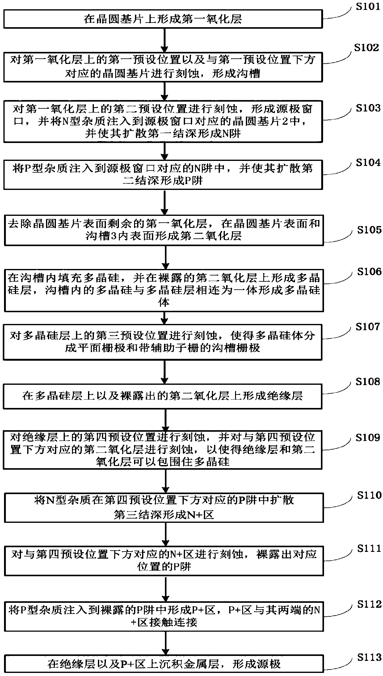
[0042] In order to solve the above-mentioned technical problems existing in the prior art, an embodiment of the present invention provides a method for manufacturing an IGBT chip with a composite gate.

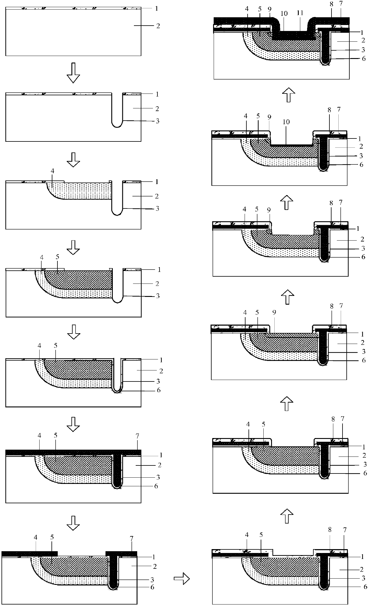
[0043] figure 1 It shows the flow chart of the method for fabricating an IGBT chip with a composite gate in Embodiment 1 of the present invention; figure 2 A schematic structural diagram showing the process of the method for manufacturing an IGBT chip with a composite gate in Embodiment 1 of the present invention.

[0044] refer to figure 1 and figure 2 , the method for fabricating an IGBT chip with a composite gate in this embodiment includes the following steps.

[0045] Step S101 , forming a first oxide layer 1 on the wafer substrate 2 .

[0046] Specifically, a uniform first oxide layer 1 is formed on the upper surface of the wafer substrate 2 by a certain method. Furthermore, the wafer substrate 2 can be a zone-melted silicon wafer, and the oxide layer can be silic...


PUM


Abstract

The invention discloses a manufacturing method for an IGBT chip with a composite grid. The method comprises the following steps: forming a first oxide layer on wafer substrate; etching a first presetposition on the first oxide layer and the wafer substrate corresponding to the lower portion of the first preset position to form a groove; re-etching to remove the first oxide layer, and forming a second oxide layer on the surface of the wafer substrate and on the inner surface of the groove; filling the groove with polysilicon, forming a polysilicon layer on the second oxide layer, and forming apolysilicon body through connecting polysilicon with the polysilicon layer in the groove into one body; and etching a third preset position on the polysilicon layer to enable the polysilicon body tobe divided into a plane grid and a groove grid with an auxiliary grid. The IGBT chip with the composite grid manufactured by the manufacturing method not only has the advantages of good voltage resistance of flat grids, but also is the advantageous in that the groove grid increases the cell density, thus greatly increasing the electric current density of the chip.

Description

technical field [0001] The invention relates to the technical field of semiconductor devices, in particular to a method for manufacturing an IGBT chip with a composite gate. Background technique [0002] Insulated gate bipolar transistor (IGBT) is a compound fully controlled voltage-driven power semiconductor device composed of bipolar transistor (BJT) and insulated gate field effect transistor (MOSFET). Due to its on-state voltage drop, the current With the characteristics of high density, high input impedance and fast response, it is widely used in rail transit, smart grid, industrial frequency conversion and new energy development and other fields. [0003] The gates of existing insulated gate bipolar transistors (IGBTs) are usually planar gates or trench gates. When the gate of the insulated gate bipolar transistor (IGBT) is a planar gate, the manufacturing process of the insulated gate bipolar transistor (IGBT) is simple, the requirements for the manufacturing equipmen...

Claims


Application Information

Patent Timeline
IPC IPC(8): H01L21/28H01L21/331H01L29/423H01L29/739H01L29/06
CPCH01L29/0615H01L29/401H01L29/42312H01L29/66325H01L29/7393
Inventor 刘国友朱春林朱利恒
Owner ZHUZHOU CRRC TIMES SEMICON CO LTD
Why Eureka
Try Eureka