Accurately controllable nano-hole manufacturing method

A manufacturing method and precise control technology, applied in nanotechnology and other directions, can solve the problems of uncertainty of use parameters, difficult to control electron beam and ion beam nanohole, etc., to achieve simple and efficient manufacturing method, wide application range, and application range wide effect

Inactive Publication Date: 2018-10-26
GUANGDONG UNIV OF TECH
View PDF5 Cites 13 Cited by
  • Summary
  • Abstract
  • Description
  • Claims
  • Application Information

AI Technical Summary

Problems solved by technology

However, due to the different types of ion beams and the uncertainty of the parameters used, it is difficult to control the formatio

Method used


Image

  • Accurately controllable nano-hole manufacturing method
  • Accurately controllable nano-hole manufacturing method
  • Accurately controllable nano-hole manufacturing method

Examples


Embodiment 1

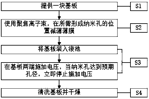
[0037] Such as figure 1 Shown is a flow chart of the precisely controlled nanopore 20 manufacturing method of the present invention, comprising the following steps:

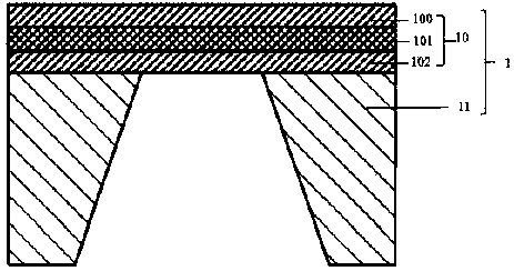
[0038] S1. Provide a substrate such as figure 2 As shown, the substrate includes a composite film 10 made of a P-type silicon chip 11 and several layers of single-layer films, and the composite film 10 is grown on one side of the P-type silicon chip 11; wherein, the back side of the P-type silicon chip 11 is photoetched and Wet etching forms an inverted cone-shaped structure, grows a 20nm silicon nitride film 102 by low-stress chemical vapor deposition on the front of the P-type silicon wafer 1111, and then grows a 20nm silicon oxide film by low-stress chemical vapor deposition 101101, and then grow a 20nm silicon nitride film 100 by low-stress chemical vapor deposition, and the back of the silicon wafer is etched into an inverted cone structure through photolithography and wet etching, exposing a 6um*6um film ...


PUM

PropertyMeasurementUnit
Thicknessaaaaaaaaaa
Minimum apertureaaaaaaaaaa

Abstract

The invention relates to the technical field of nanofabrication, in particular to an accurately controllable nano-hole manufacturing method which includes the steps: firstly, providing a substrate andthinning a film at a position needing to form nano-holes by a focusing ion beam; secondly, placing the substrate into a liquid tank; applying voltage to two ends of the substrate and stopping applying the voltage when the nano-holes reach expected hole diameters; finally, cleaning and drying the substrate to obtain the nano-holes with accurately controllable positions and sizes. The nano-holes can be formed in a micron-sized or nano-sized multilayer composite film, and the applicable range is wide. The film is thinned at the position needing to form the nano-holes by the focusing ion beam, sothat the nano-holes are formed in the thinned position and can be accurately positioned. Moreover, the nano-holes with the hole diameters smaller than 10nm are finally formed by electric breakdown, the hole diameters of the nano-holes are continuously enlarged along with continuous voltage application and can be accurately controlled according to real-time voltage and real-time current, and the nano-holes with the needed hole diameters are accurately manufactured.

Description

technical field [0001] The present invention relates to the technical field of nano-processing, and more specifically, relates to a precisely controlled nano-hole manufacturing method. Background technique [0002] In the past 20 years, nanopore technology has attracted great attention and has become an important research topic due to its low-cost label-free single-molecule DNA testing. In addition, another advantage of using nanopores for DNA testing lies in the possibility of reading long DNA sequences. The use of nanopores for DNA testing is crucial for providing personalized medicine and early detection of cancer in the future. The current nanopore technology can be roughly divided into two categories: one is "biological nanopore" related to biological materials, and the other is "solid-state nanopore" related to semiconductor materials. The most common DNA sequencing method used jointly by biological nanopores and solid-state nanopores is to detect changes in the ionic...

Claims


Application Information

Patent Timeline
IPC IPC(8): B82Y40/00
CPCB82Y40/00
Inventor 袁志山雷鑫刘佑明王成勇
Owner GUANGDONG UNIV OF TECH
Why Eureka
Try Eureka