Scalable chip architecture of tile-type TR component millimeter wave

An extended architecture, millimeter-wave technology, applied in the direction of electrical components, antenna support/mounting devices, antenna arrays, etc., can solve the problems of inconsistent heat dissipation paths of radio frequency channels, large longitudinal dimensions of TR components, and high single-channel chips. The contradiction between layout space and chip integration, the effect of reducing chip-level integration costs and increasing functional density and channel density

Inactive Publication Date: 2018-11-06
10TH RES INST OF CETC
View PDF7 Cites 4 Cited by
  • Summary
  • Abstract
  • Description
  • Claims
  • Application Information

AI Technical Summary

Problems solved by technology

With the technological leap from single-function to single-chip multi-function of semiconductor radio frequency chips, brick-type TR components gradually cover the engineering application requirements of millimeter-wave two-dimensional active phased arrays below the Ka frequency band, but the brick-type architecture exposes inadequacies in applications. Few problems: single-channel chips occupy a high proportion, such as the current relatively high integration "two-chip" solution (transmitter chip + amplitude-phase modulation core chip), the number of single-channel chips is still more than two, and the area exceeds 12mm 2 , making it difficult to significantly reduce the cost of TR components; since the link function is spread along the Z direction, the longitudinal size of TR components is relatively large, and it is difficult to meet the low profile and thinner requirements required by miniaturized antennas in the millimeter wave frequency band; the main heat exchange area of ​​TR components Located on the periphery, the heat dissipation paths of each RF channel are inconsistent, especially in high-power applications, there will be a high temperature gradient, which will affect the performance and stability of the chip
Although SOC (System-On-Chip) of TR component chips is the first choice under the condition of only focusing on chip integration and single-channel chip area, it is still difficult to find a combination of Powerful digital-analog hybrid integration capabilities, large-scale low-cost production, and an all-round semiconductor process with excellent radio frequency performance mean that the SOC solution will inevitably pay a price in terms of performance and cost. will counteract the cost

Method used


Image

  • Scalable chip architecture of tile-type TR component millimeter wave
  • Scalable chip architecture of tile-type TR component millimeter wave

Examples


Embodiment Construction

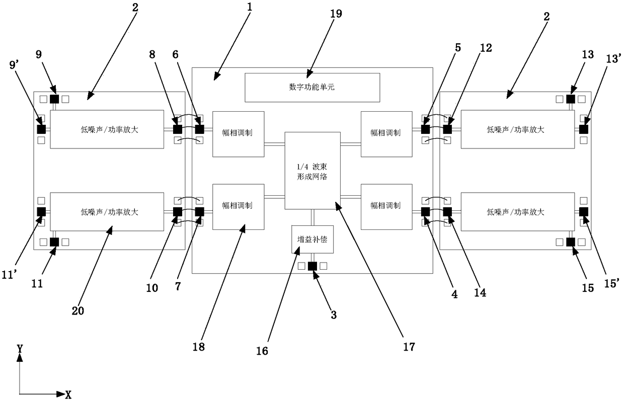
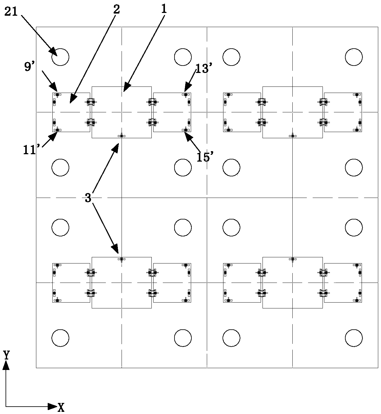
[0016] See figure 1 , figure 2 . In the embodiment described below, a tile-type TR module millimeter wave chip scalable architecture includes: gapless assembly on the XY plane, an amplitude-phase modulation chip 1 that integrates multiple digital-analog mixing functions, and dual-channel parallel integration The layout of the multifunctional chip 2; among them, the amplitude-phase modulation chip 1 has four amplitude-phase modulation channels symmetrical, and the one-to-four power distribution synthesis network 17 arranged in the center of the amplitude-phase modulation chip 1 corresponds to the four-channel amplitude-phase modulation channel connection amplitude and phase The modulation unit 18, the one-to-four power distribution synthesis network 17 is connected to the radio frequency port 3 of the antenna beam forming network docking common port through the connected common channel gain compensation unit 16, and the radio frequency port 3 is provided with a digital function...


PUM


Abstract

The scalable chip architecture of tile-type TR component millimeter wave proposed by the invention aims to provide the universal, reliable, flexibly extensible and low-cost chip architecture with highfunctional density and channel integration density. The invention is realized by the following technical solutions: four paths of amplitude-phase modulation channels of the amplitude-phase modulationchip are bilaterally symmetric, the one-divide-into-four power distribution synthesis network disposed in the center of the amplitude-phase modulation chip is connected to the amplitude-phase modulation unit corresponding to the four paths of amplitude-phase modulation channels, the one-divide-into-four power distribution synthesis network is connected to the radio frequency port of the docked common port of the antenna beamforming network by the connected common channel gain compensation unit, the opposite sides of the radio frequency port are provided with digital function units, and the four symmetric amplitude-phase modulation units are symmetrically connected to the low-noise / power amplification unit in the multifunctional chip respectively through the four-channel radio frequency ports correspondingly connected at left and right sides of the amplitude-phase modulation chip, thereby forming an expandable basic unit that communicates with respectively corresponding sub-array antenna interconnecting radio frequency interfaces.

Description

Technical field [0001] The invention relates to an expandable chip architecture that can be widely used in millimeter wave phased array antenna TR components in various fields such as communications, radar, guidance, remote sensing, spectrum science, and biological effects. The so-called "phased array" refers to the regular arrangement of thousands of radiating elements on the antenna, and the phase of each radiating element is regularly controlled. Background technique [0002] The two-dimensional active phased array antenna, with its scanning beam without inertial agility, excellent radio frequency performance, and good channel redundancy, has been rapidly developed and widely used in recent years. The biggest feature of this type of antenna is that the active transceiver channel of the TR component is set at 1 / 2λ in a two-dimensional plane. g The (working wavelength) spacing is periodically expanded, which also forms the most basic and most important constraint in the layout o...

Claims


Application Information

Patent Timeline
Patent Type & Authority Applications(China)
IPC IPC(8): H01Q1/12H01Q21/00H01Q23/00
CPCH01Q1/12H01Q21/00H01Q23/00
Inventor 张凯
Owner 10TH RES INST OF CETC
Why Eureka
Try Eureka