A kind of zno nanometer material, and preparation method thereof
A technology of nanomaterials and nanowires, which is applied in the field of ZnO nanomaterials and its preparation, can solve the problems of insignificant advantages of electrode materials, excessive macroscopic size, complex preparation process, etc., and achieve mature preparation equipment, simple process, and convenient scale The effect of chemical production
- Summary
- Abstract
- Description
- Claims
- Application Information
AI Technical Summary
Problems solved by technology
Method used
Image
Examples
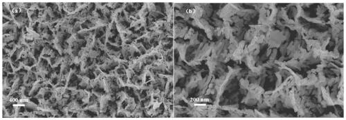
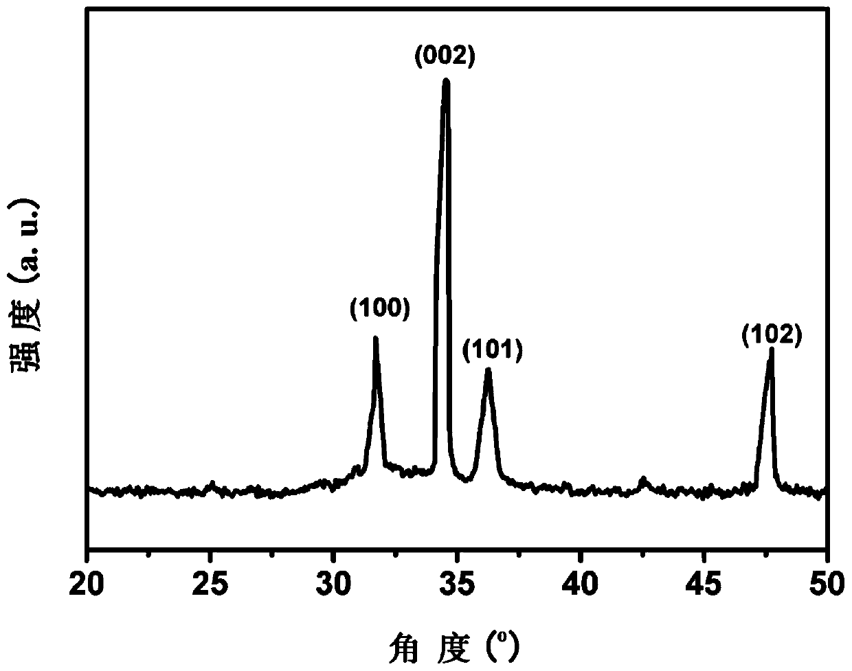
Embodiment 1
[0030] A preparation method of ZnO nanometer material, comprising the following steps:
[0031] 1), the preparation of the precursor mixed solution, the pore-forming agent polyethylene oxide-polypropylene oxide-polyethylene oxide triblock copolymer and zinc acetate were added to 10mL according to the mass ratio of 0.5:100 In ethylene glycol, magnetically stirred at 60°C for 60min to obtain a clear precursor mixed solution;
[0032] 2) For the preparation of the precursor thin film, place the substrate on a spin coater, first drop 2 drops of the precursor mixed solution on the center of the substrate, and then rotate at 500 rpm for 30s to spread the mixed solution on the substrate ;
[0033] 3), then, rotate at 1500 rpm for 100s;
[0034] 4), then, rotate at 3000 rpm for 120s to obtain a uniformly distributed precursor film;
[0035] 5), high temperature sintering, transfer the precursor film prepared in step 4) to a box-type annealing furnace, start from room temperature, r...
Embodiment 2
[0039] A preparation method of ZnO nanometer material, comprising the following steps:
[0040] 1), the preparation of the precursor mixed solution, the pore-forming agent polyethylene oxide-polypropylene oxide-polyethylene oxide triblock copolymer and zinc acetate were added to 25mL according to the mass ratio of 0.5:100 In ethylene glycol, magnetically stirred at 80°C for 80min to obtain a clear precursor mixed solution;
[0041] 2) For the preparation of the precursor thin film, place the substrate on a spin coater, first drop 4 drops of the precursor mixed solution in the center of the substrate, and then rotate at 500 rpm for 50s to spread the mixed solution on the substrate ;
[0042] 3), then, rotate at 2000 rpm for 30s;
[0043] 4), then, rotate at 4000 rpm for 60s to obtain a uniformly distributed precursor film;
[0044] 5), high temperature sintering, transfer the precursor film prepared in step 4) to a box-type annealing furnace, start from room temperature, rai...
Embodiment 3
[0047] Application of ZnO Nanomaterials in Photodetectors
[0048] On the ZnO nanomaterial prepared in Example 1, continue to epitaxially grow the Au electrode, thereby preparing a photodetector, specifically: use a mask plate and an electron beam to evaporate the metal Au electrode, and form an ohmic contact and a Schottky junction after annealing, The photodetector consists of ZnO nanomaterials and metal Au electrodes, and its structure is as Figure 4 As shown, the dark current of the prepared ZnO nanomaterial photodetector is only 30.2pA under 1V bias, and the maximum value of the device reaches 0.874A / W under 1V bias.
PUM
| Property | Measurement | Unit |
|---|---|---|
| diameter | aaaaa | aaaaa |
| conversion efficiency | aaaaa | aaaaa |
Abstract
Description
Claims
Application Information


