Medium cavity substrate integration waveguide structure based on silicon through hole technology and manufacturing technology thereof

A substrate-integrated waveguide and dielectric cavity technology, which is applied in waveguides, waveguide-type devices, circuits, etc., can solve the problems of large loss and hinder the wide application of substrate-integrated waveguides, and achieve the effect of improving resonance extraction

Inactive Publication Date: 2018-11-16
XIDIAN UNIV
View PDF6 Cites 10 Cited by
  • Summary
  • Abstract
  • Description
  • Claims
  • Application Information

AI Technical Summary

Problems solved by technology

However, due to the large loss of the semiconductor silicon substrate at high frequencies, it hinders the wide application of the substrate-integrated waveguide (SIW) structure in three-dimensional integration.

Method used


Image

  • Medium cavity substrate integration waveguide structure based on silicon through hole technology and manufacturing technology thereof

Examples


Embodiment Construction

[0041] The present invention will be specifically introduced below in conjunction with the accompanying drawings and specific embodiments.

[0042] Firstly, the dielectric cavity substrate integrated waveguide structure based on the through-silicon via technology of the present invention is introduced.

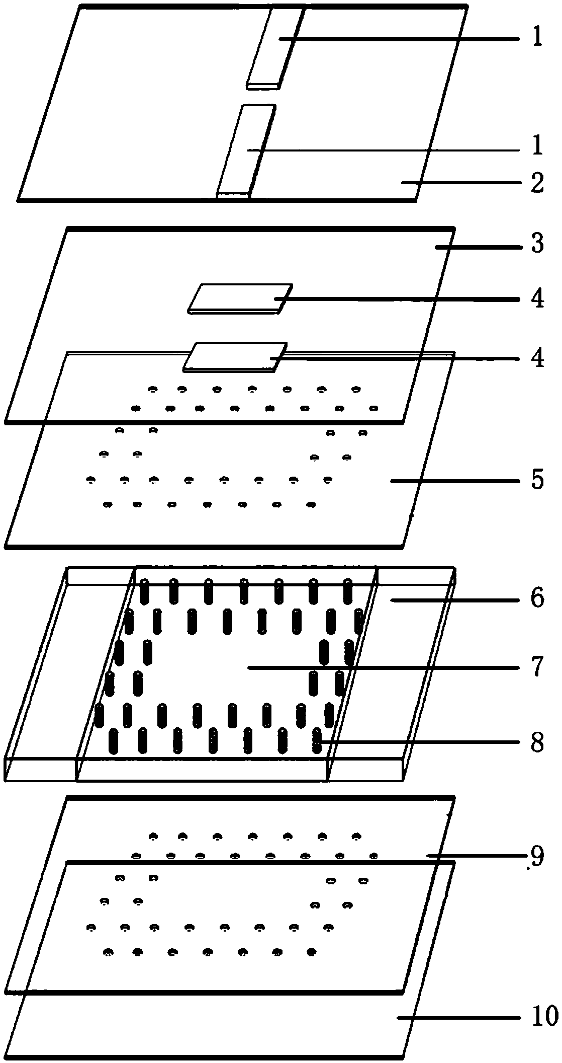
[0043] refer to figure 1, the dielectric cavity substrate integrated waveguide (SIW) structure based on through-silicon via technology of the present invention, which comprises from top to bottom: a top metal interconnect dielectric layer 2, a top ground ground plate 3, and an intermediate metal interconnect dielectric layer 5 , a low-resistance silicon substrate 6 , a bottom metal interconnection dielectric layer 9 and a bottom ground plane 10 .

[0044] 1. The top metal interconnect dielectric layer

[0045] The top metal interconnect dielectric layer 2 is used to electrically isolate the top ground plane 3 from other metal interconnects, and it uses insulating materials s...


PUM

PropertyMeasurementUnit
thicknessaaaaaaaaaa

Abstract

The invention discloses a medium cavity substrate integration waveguide structure based on a silicon through hole technology and a manufacturing technology thereof. A TSV three-dimensional packaging technology is used to integrate the substrate integration waveguide (SIW) structure into a three-dimensional chip system with a small volume. In the structure, a silicon substrate around TSV metal conductor columns is etched and a medium between the TSV metal conductor columns is changed into a high-molecular polymer benzocyclobutene (BCB) insulation material with a low dielectric constant from a low-resistance silicon substrate so that the eddy current effect of the silicon substrate in a high frequency circuit is eliminated, the corresponding high frequency losses of the silicon substrate donot exist, the power consumption of the substrate integration waveguide (SIW) structure of the invention is further reduced and a quality factor is increased. The resonant extraction of the substrateintegration waveguide (SIW) structure of the invention is greatly improved by the introduction of low-consumption high-molecular polymer benzocyclobutene (BCB) (filled in a BCB medium cavity).

Description

technical field [0001] The invention relates to a substrate-integrated waveguide structure and its preparation process, in particular to a dielectric cavity-substrate-integrated waveguide structure based on through-silicon via technology and its preparation process, belonging to integrated circuit manufacturing, integrated circuit packaging and microsystem packaging technologies field. Background technique [0002] In recent years, driven by commercial applications, mmWave wireless communication has developed rapidly, such as short-range point-to-point high data rate wireless communication, passive imaging systems, and automotive radar. These applications all require millimeter-wave wireless communication systems to have high performance, miniaturization, high integration, and (most importantly) low production costs. In order to achieve a high degree of integration and the smallest overall device volume, the system-on-chip (SoC) has become the focus of people's research. So...

Claims


Application Information

Patent Timeline
Patent Type & Authority Applications(China)
IPC IPC(8): H01P3/16
CPCH01P3/16
Inventor 刘晓贤朱樟明杨银堂丁瑞雪李跃进
Owner XIDIAN UNIV
Why Eureka
Try Eureka