Probe micro displacement sensing system based on surface nanoscale axial photonics structure echo wall microcavity
A technology of displacement sensing system and photon structure, which is applied in the field of optical sensing, can solve the problems of affecting the sensing accuracy, complicated devices, and difficulty in probe-type measurement of the system, and achieves high sensing accuracy, easy packaging, and guaranteed system The effect of stability
- Summary
- Abstract
- Description
- Claims
- Application Information
AI Technical Summary
Problems solved by technology
Method used
Image
Examples
Embodiment 1
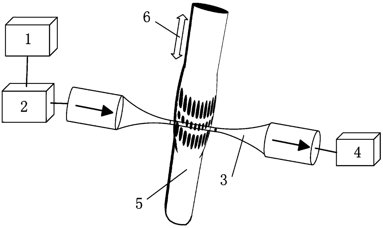
[0028] figure 1 It is a schematic structural diagram of the probe-type micro-displacement sensing system based on the SNAP structure microcavity proposed by the present invention. In order to express the principle of the system more clearly, the dimensions and proportions of all the devices in the figure do not follow the real scale, which is hereby explained. The system includes a tuning laser 1 , a polarization controller 2 , a coupling waveguide 3 , a photodetector 4 , a SNAP structure microcavity 5 and a displacement device 6 . Among them, the tuned laser 1 generates continuous, wavelength-tunable laser and inputs it into the optical fiber; the polarization controller 2 controls the polarization state of the light in the optical fiber; the coupling waveguide 3 is used to couple the light wave into the microcavity of the SNAP structure; the photodetector 4 is used for It is used to convert the optical signal into an electrical signal to obtain the resonance spectrum of the ...
Embodiment 2
[0033] In this embodiment, the working wavelength of the tuned laser 1 is around 1550nm, and the linewidth is 300kHz; the coupling waveguide 3 is a polished angled optical fiber, which is obtained by high-precision grinding of the end face of a conventional optical fiber; the SNAP structure microcavity 5 is obtained by carbon dioxide laser processing, Its axial length is about 300 μm, the radial direction is Gaussian curve shape, and the maximum radius change is about 15 nm.
Embodiment 3
[0035] In this embodiment, the working wavelength of the tuning laser 1 is around 1550nm, and the line width is 300kHz; the coupling waveguide 3 is an integrated optical waveguide, which is obtained by photolithography; the SNAP structure microcavity 5 is obtained by ultraviolet laser processing, and its axial length is about 400 μm , the radial direction is trapezoidal, and the maximum radius changes about 10nm.
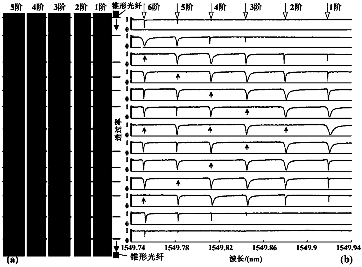
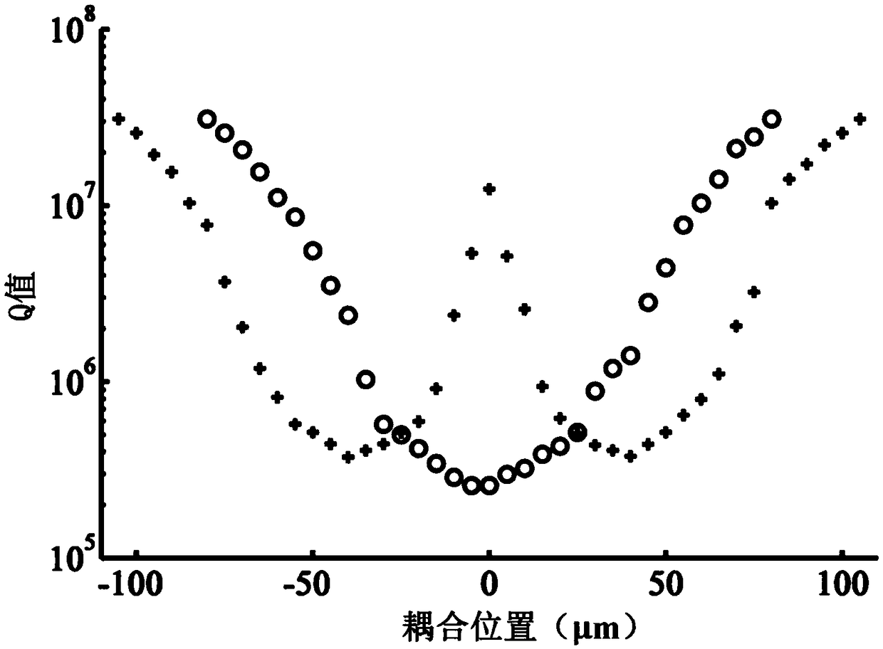
[0036] In summary, the present invention proposes a micro-displacement sensing system that can realize probe-type measurement. The system is based on the mode field distribution and mode spectrum structure characteristics of the whispering gallery microcavity with the SNAP structure. The characteristics of the characteristic parameters of each axial mode change, and the sensing of the axial displacement of the microcavity is realized by measuring the Q value and transmittance of each mode in the resonance spectrum. During the working process, the microcavity of the ...
PUM
 Abstract
Description
Claims
Application Information


