Supercharge Your Innovation With Domain-Expert AI Agents!

Gallium nitride-based high electron mobility transistor

A high electron mobility, gallium nitride-based technology, applied in the field of gallium nitride-based high electron mobility transistors, can solve the problem of increased device on-resistance, reduced device buffer layer leakage current, and limited increase in device breakdown voltage, etc. problem, to achieve the effect of ensuring the operating frequency and switching speed, optimizing the distribution of the transverse electric field, and ensuring the forward current capability

Active Publication Date: 2018-11-23
UNIV OF ELECTRONICS SCI & TECH OF CHINA
View PDF5 Cites 6 Cited by
  • Summary
  • Abstract
  • Description
  • Claims
  • Application Information

AI Technical Summary

Problems solved by technology

However, the activation rate of P-GaN is very low, and the effect of improving the withstand voltage capability of the device is limited
[0007] 3. Use AlGaN and other back barrier buffer layer structures, mentioned in the literature [Oliver Gilt et al. "Normally-offAlGaN / GaN HFET with p-type GaN Gate and AlGaN Buffer", Integrated PowerElectronics Systems, 2010], AlGaN and other back potential The use of the barrier increases the barrier height from the channel two-dimensional electron gas to the buffer layer, thereby reducing the leakage current of the device buffer layer. However, this technology also has a limited improvement in the breakdown voltage of the device and fails to fully reflect the potential of gallium nitride. The advantage of the withstand voltage of the material; at the same time, the AlGaN back barrier will not only introduce traps due to lattice mismatch between the buffer layer and the channel layer, but also because AlGaN in the buffer layer and AlGaN in the barrier layer have opposite polarization effects, On the contrary, it will reduce the two-dimensional electron gas concentration in the channel, which will lead to an increase in the on-resistance of the device.

Method used


Image

  • Gallium nitride-based high electron mobility transistor
  • Gallium nitride-based high electron mobility transistor
  • Gallium nitride-based high electron mobility transistor

Examples


Embodiment 1

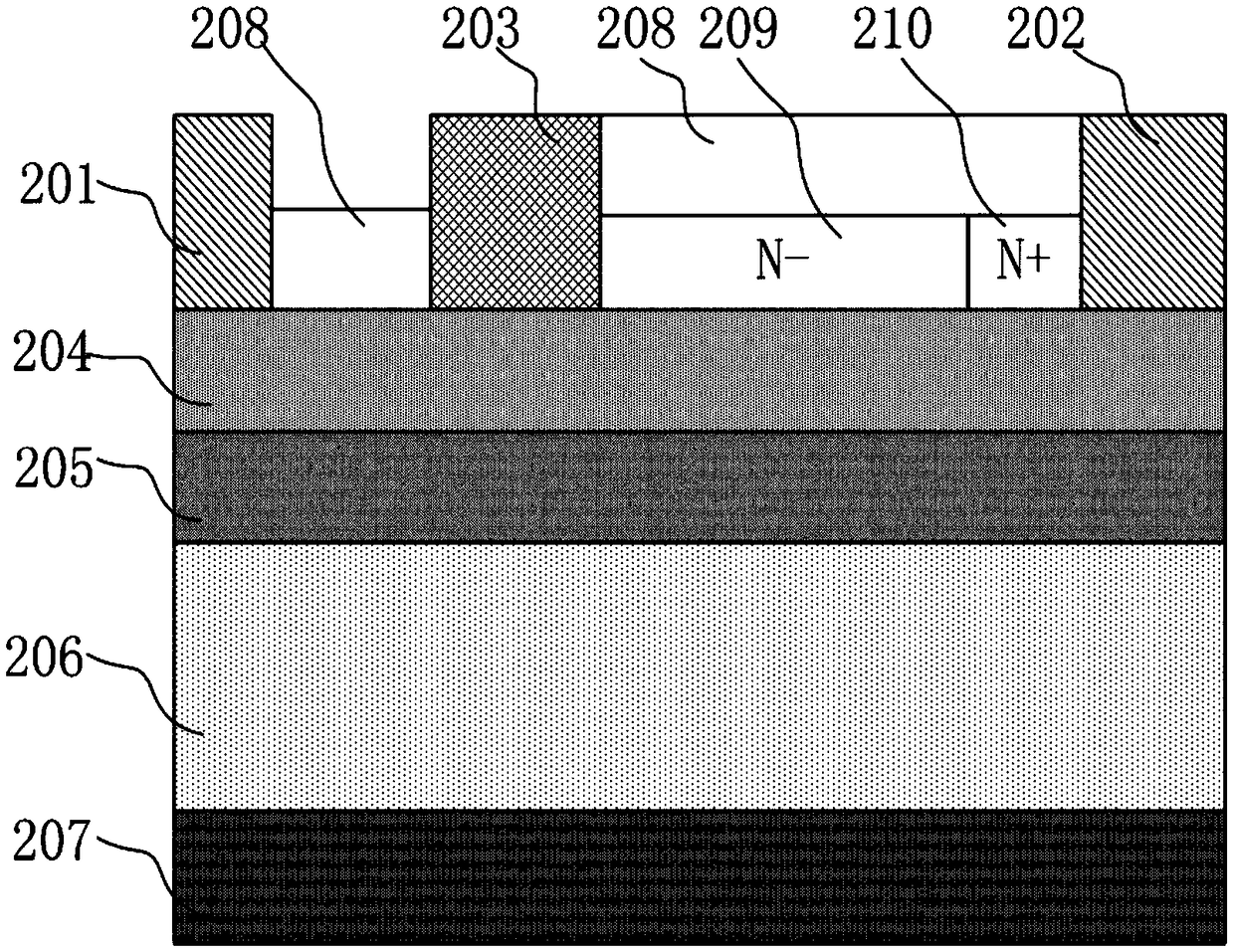
[0032] This embodiment provides a GaN-based high electron mobility transistor, such as figure 2 As shown, it includes a substrate 207, a gallium nitride buffer layer 206, a gallium nitride channel layer 205, an aluminum gallium nitride barrier layer 204, and a substrate 207 disposed on the aluminum gallium nitride barrier layer 204, which are sequentially stacked from bottom to top. The source electrode 201, the drain electrode 202 and the gate electrode 203 on the surface; the molecular formula of the aluminum gallium nitrogen barrier layer 204 in this embodiment is Al x Ga y N, where 0≤x≤1, 0≤y≤1, x+y=1; both the source 201 and the drain 202 form ohmic contacts with the AlGaN barrier layer 204, and the gate The electrode 203 forms a Schottky contact with the AlGaN barrier layer 204; it is characterized in that: the upper surface of the AlGaN barrier layer 204 between the gate 203 and the drain 202 is provided with N-type semiconductors in contact with each other layer 209...

Embodiment 2

[0034] This embodiment provides a GaN-based high electron mobility transistor, such as image 3 As shown, it includes a substrate 307, a gallium nitride buffer layer 306, a gallium nitride channel layer 305, an aluminum gallium nitride barrier layer 304, and an aluminum gallium nitride barrier layer 304 that are stacked sequentially from bottom to top. The source electrode 301, the drain electrode 302 and the gate electrode 303 on the surface; the molecular formula of the aluminum gallium nitrogen barrier layer 204 in this embodiment is Al x Ga y N, where 0≤x≤1, 0≤y≤1, x+y=1; both the source 301 and the drain 302 form an ohmic contact with the AlGaN barrier layer 304, and the gate The electrode 303 forms a Schottky contact with the AlGaN barrier layer 304; it is characterized in that: the upper surface of the AlGaN barrier layer 304 between the gate 303 and the drain 302 is provided with N - IN + structure, the N - IN + The structure includes an N-type semiconductor layer...

Embodiment 3

[0036] This embodiment adopts as figure 2 The shown device structure is subjected to a two-dimensional numerical simulation test. In order to compare the performance of the present invention with a traditional GaN HEMT device, this embodiment adopts a traditional method with the same parameters except that the N-type semiconductor layer 209 and the N+ type semiconductor layer 210 are not introduced. A GaN HEMT device was used as a comparative example. The structural parameters used for device simulation are shown in Table 1 below:

[0037] Table 1 Device Simulation Structure Parameters

[0038]

[0039]

[0040] Such as Figure 4 and Figure 5 As shown, the simulation results of this embodiment fully demonstrate the advantages of the present invention. from Figure 4 It can be seen that the specific embodiment of the present invention proposes that the breakdown voltage value of the GaN HEMT device is 1354V, while the breakdown voltage value of the common GaN HEMT ...


PUM


Abstract

The invention discloses a gallium nitride-based high electron mobility transistor, and belongs to the technical field of semiconductor devices. According to the transistor, a transverse schottky diodewith a rectifying effect is formed between a grid electrode and a drain electrode of a conventional GaN HEMT device to be used as a voltage-resistant structure, so that the surface electric field ofa component is modulated, and the distribution of a transverse electric field is optimized, thereby achieving the purpose of improving the breakdown voltage of the device; meanwhile, the existence ofthe transverse schottky diode can also bear certain reverse voltage in a blocking state, and the grid electrode is prevented from generating too large leakage current when the grid electrode is subjected to positive voltage under the positive conducting state, so that the forward current capability of the device is guaranteed; and in addition, compared with a field plate structure, additional parasitic capacitance is not introduced, so that the working frequency and the switching speed of the device are ensured, and the reliability of the device is improved.

Description

technical field [0001] The invention belongs to the technical field of semiconductor devices, and in particular relates to a GaN-based high electron mobility transistor with a lateral Schottky diode withstand voltage structure. Background technique [0002] Gallium nitride (GaN)-based high electron mobility transistors have excellent characteristics such as large band gap, high critical breakdown electric field, high electron saturation velocity, good thermal conductivity, radiation resistance and good chemical stability. GaN) materials can form a two-dimensional electron gas heterojunction channel with high concentration and high mobility with materials such as aluminum gallium nitride (AlGaN) or indium gallium nitride (InGaN). Therefore, gallium nitride (GaN)-based high electron Mobility transistors are especially suitable for high-voltage, high-power and high-temperature applications, and have become one of the most potential transistors for power electronics applications...

Claims


Application Information

Patent Timeline
Patent Type & Authority Applications(China)
IPC IPC(8): H01L29/778H01L21/335H01L29/06
CPCH01L29/0684H01L29/083H01L29/66462H01L29/778
Inventor 杜江锋汪浩刘勇白智元辛奇于奇
Owner UNIV OF ELECTRONICS SCI & TECH OF CHINA
Features
  • R&D
  • Intellectual Property
  • Life Sciences
  • Materials
  • Tech Scout
  • Unparalleled Data Quality
  • Higher Quality Content
  • 60% Fewer Hallucinations
Learn More