Efficient two-dimensional superlattice heterojunction photovoltaic device and preparation thereof

A photovoltaic device and superlattice technology, applied in the field of efficient two-dimensional superlattice heterojunction photovoltaic devices and their preparation, can solve problems such as being unsuitable for multi-layer periodic superlattice, and achieve excellent mobility and stability properties, weakening interlayer coupling, and high light absorption efficiency

Active Publication Date: 2018-11-27
SHANGHAI UNIVERSITY OF ELECTRIC POWER
View PDF4 Cites 6 Cited by
  • Summary
  • Abstract
  • Description
  • Claims
  • Application Information

AI Technical Summary

Problems solved by technology

But not suitable for multilayer periodic superlattice construction

Method used


Image

  • Efficient two-dimensional superlattice heterojunction photovoltaic device and preparation thereof
  • Efficient two-dimensional superlattice heterojunction photovoltaic device and preparation thereof

Examples


Embodiment 1

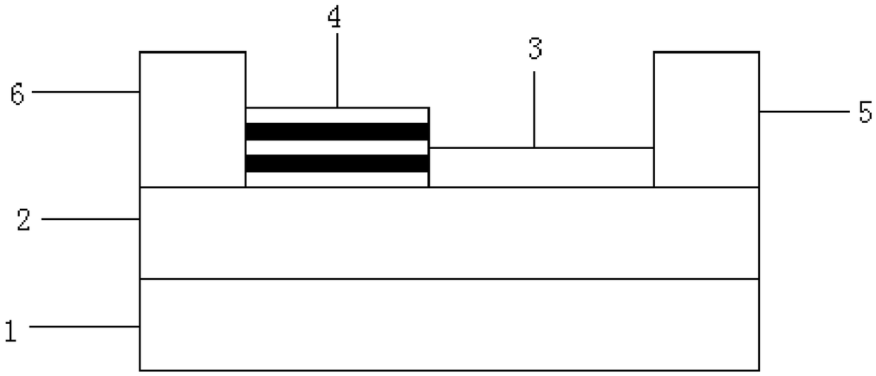
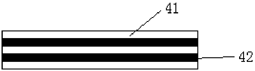
[0029] A high-efficiency two-dimensional superlattice heterojunction photovoltaic device with a structure such as figure 1 As shown, it at least includes a substrate 1, a silicon dioxide layer 2 grown on the substrate 1, and a multi-layer two-dimensional material covered on the silicon dioxide layer, and each layer in the multi-layer two-dimensional material part area Organic molecular layers are embedded between them to form a two-dimensional superlattice structure 4. The two-dimensional superlattice structure 4 is composed of a two-dimensional material layer 41 and an embedded organic molecular layer 42. Its structure is as follows figure 2 As shown, the two-dimensional superlattice structure 4 and the multi-layer two-dimensional material 3 not embedded in the organic molecular layer 42 form a two-dimensional superlattice heterostructure, and two ends of the two-dimensional superlattice heterostructure are respectively grown with metal electrode.

[0030] The preparation m...

Embodiment 2

[0038] A highly efficient two-dimensional superlattice heterojunction photovoltaic device, the structure of which is the same as in Example 1, except that the preparation method is changed to:

[0039] First, polysilicon is used as the substrate material, and a silicon dioxide film is grown on the substrate layer with a thickness of 100 nm.

[0040] Then, a layer of black phosphorus is adopted by mechanical peeling method, and the black phosphorus is multi-layered with a thickness of more than 2.5nm. It is then transferred onto the silicon dioxide layer by transfer technology.

[0041] Afterwards, a layer of photoresist is covered on the part of the black phosphorus.

[0042] Then, the device structure composed of polysilicon, silicon dioxide and black phosphorus was immersed in an electrolyte solution of tetrabutylammonium bromide.

[0043] Subsequently, a working electrode, a counter electrode and a reference electrode were fabricated. The working electrode material is pl...

Embodiment 3-7

[0047] The difference from Example 1 is that in this example, the multilayer two-dimensional materials are replaced by molybdenum disulfide, tungsten diselenide, indium selenide, tin selenide or germanium sulfide.


PUM

PropertyMeasurementUnit
thicknessaaaaaaaaaa
thicknessaaaaaaaaaa
thicknessaaaaaaaaaa

Abstract

The invention relates to an efficient two-dimensional superlattice heterojunction photovoltaic device and preparation thereof. The preparation method of the efficient two-dimensional superlattice heterojunction photovoltaic device includes the steps: a) immersing a device structure composed of a substrate (1), a silicon dioxide layer (2) and multiple layers of two-dimensional materials into an electrolyte solution containing organic molecules; b) preparing a three-electrode system on the multiple layers of two-dimensional materials and applying a negative voltage to insert organic molecules with positive charges into part of the region of the multiple layers of two-dimensional materials to form a two-dimensional superlattice structure (4), and then obtaining a two-dimensional superlatticeheterostructure; and c) finally, growing metal electrodes at both ends of the two-dimensional superlattice heterostructure, thus completing the preparation process. Compared with the prior art, the present invention discloses stable superlattice materials in which two-dimensional materials and organic molecular layers alternate with each other. The superlattice materials and the two-dimensional multilayer material constitute a heterojunction photovoltaic device, and the result is equivalent to parallel connection of a plurality of two-dimensional material heterojunctions, and the light absorption efficiency is high, and the mobility and the stability are high.

Description

technical field [0001] The invention belongs to the technical field of semiconductor devices, and relates to a high-efficiency two-dimensional superlattice heterojunction photovoltaic device and its preparation. Background technique [0002] Two-dimensional nanomaterials have become a new generation of high-performance nanomaterials and one of the core materials of international frontier research. Single-layer MoS 2 For example, its electron mobility can reach 200cm at room temperature 2 / Vs. At the same time, when obtaining the same effect of electron movement, MoS 2 Thinner and lighter than Si. It consumes 100,000 times less power than Si transistors in steady state. At the same time MoS 2 With a direct bandgap, using MoS 2 The fabricated light-emitting device has excellent photoelectric properties. Also based on MoS 2 With its flexible characteristics, the device can be bent and stretched, thus giving birth to many new application fields. If different types of o...

Claims


Application Information

Patent Timeline
Patent Type & Authority Applications(China)
IPC IPC(8): H01L51/42H01L51/46H01L51/48
CPCH10K71/12H10K30/10H10K2102/00Y02E10/549
Inventor 汤乃云
Owner SHANGHAI UNIVERSITY OF ELECTRIC POWER
Why Eureka
Try Eureka