
Silicon-based SERS chip DNA database constructing and training method used for artificial intelligence detection of DNA

A DNA database and artificial intelligence technology, applied in the field of DNA sensing technology, can solve problems such as poor signal reproducibility and weak SERS signal strength, and achieve good specificity, convenient detection process, and safe operation

Active Publication Date: 2018-11-30
SUZHOU UNIV
View PDF3 Cites 1 Cited by
  • Summary
  • Abstract
  • Description
  • Claims
  • Application Information

AI Technical Summary

Problems solved by technology

These issues lead to weaker or less reproducible SERS signals

Method used


Image

  • Silicon-based SERS chip DNA database constructing and training method used for artificial intelligence detection of DNA
  • Silicon-based SERS chip DNA database constructing and training method used for artificial intelligence detection of DNA
  • Silicon-based SERS chip DNA database constructing and training method used for artificial intelligence detection of DNA

Examples


Embodiment 1

[0062] Take 0.5cm 2 Put 3-6 monocrystalline silicon wafers of different sizes into a clean beaker and ultrasonically clean them with deionized water and acetone for 15 minutes respectively, and then put them into a mixed solution of 40mL concentrated sulfuric acid and hydrogen peroxide to remove the hard surface. Dissolved impurities are finally cleaned with deionized water to obtain a clean silicon wafer.

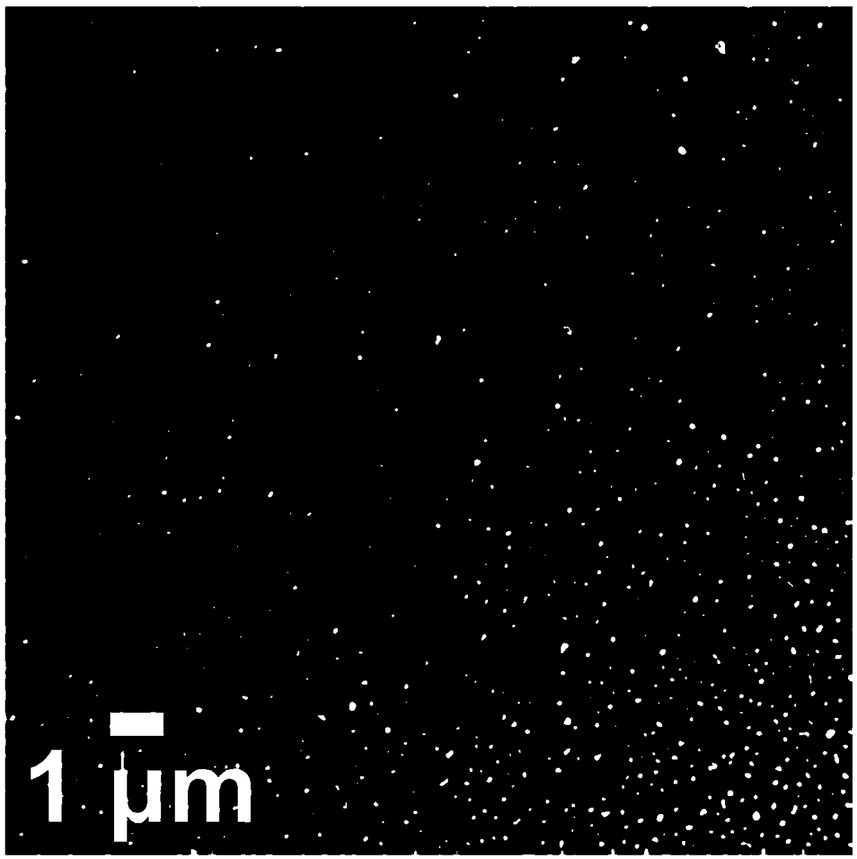
[0063] Put the cleaned silicon chip into a hydrofluoric acid solution (mass concentration: 5%) for hydrosilylation reaction for 30 minutes, so that the surface of the silicon chip is covered with a large number of Si—H bonds. Place the treated silicon chip in a petri dish with the shiny side up, add silver nitrate (1M) and hydrogen fluoride (mass concentration: 40%) in a mixed solution (volume ratio = 1:50) for reduction reaction for 60 minutes, according to The principle of electrochemical reaction is that silver ions are reduced by Si-H bonds, and a layer of uniform sil...

Embodiment 2

[0067] Take 0.5cm 2 Put 3-6 monocrystalline silicon wafers of different sizes into a clean beaker and ultrasonically clean them with deionized water and acetone for 15 minutes respectively, and then put them into a mixed solution of 40mL concentrated sulfuric acid and hydrogen peroxide to remove the hard surface. Dissolved impurities are finally cleaned with deionized water to obtain a clean silicon wafer.

[0068] Put the cleaned silicon chip into a hydrofluoric acid solution (mass concentration: 5%) for hydrosilylation reaction for 30 minutes, so that the surface of the silicon chip is covered with a large number of Si—H bonds. Place the treated silicon chip in a petri dish with the shiny side up, add silver nitrate (1M) and hydrogen fluoride (mass concentration: 40%) in a mixed solution (volume ratio = 1:50) for reduction reaction for 60 minutes, according to The principle of electrochemical reaction is that silver ions are reduced by Si-H bonds, and a layer of uniform sil...

Embodiment 3

[0072] Take 0.5cm 2 Put 3-6 monocrystalline silicon wafers of different sizes into a clean beaker and ultrasonically clean them with deionized water and acetone for 15 minutes respectively, and then put them into a mixed solution of 40mL concentrated sulfuric acid and hydrogen peroxide to remove the hard surface. Dissolved impurities are finally cleaned with deionized water to obtain a clean silicon wafer.

[0073] Put the cleaned silicon chip into a hydrofluoric acid solution (mass concentration: 5%) for hydrosilylation reaction for 30 minutes, so that the surface of the silicon chip is covered with a large number of Si—H bonds. Place the treated silicon chip in a petri dish with the shiny side up, add silver nitrate (1M) and hydrogen fluoride (mass concentration: 40%) in a mixed solution (volume ratio = 1:50) for reduction reaction for 60 minutes, according to The principle of electrochemical reaction is that silver ions are reduced by Si-H bonds, and a layer of uniform sil...


PUM


Abstract

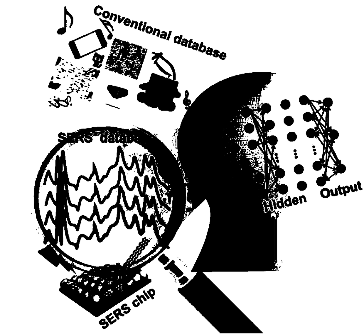
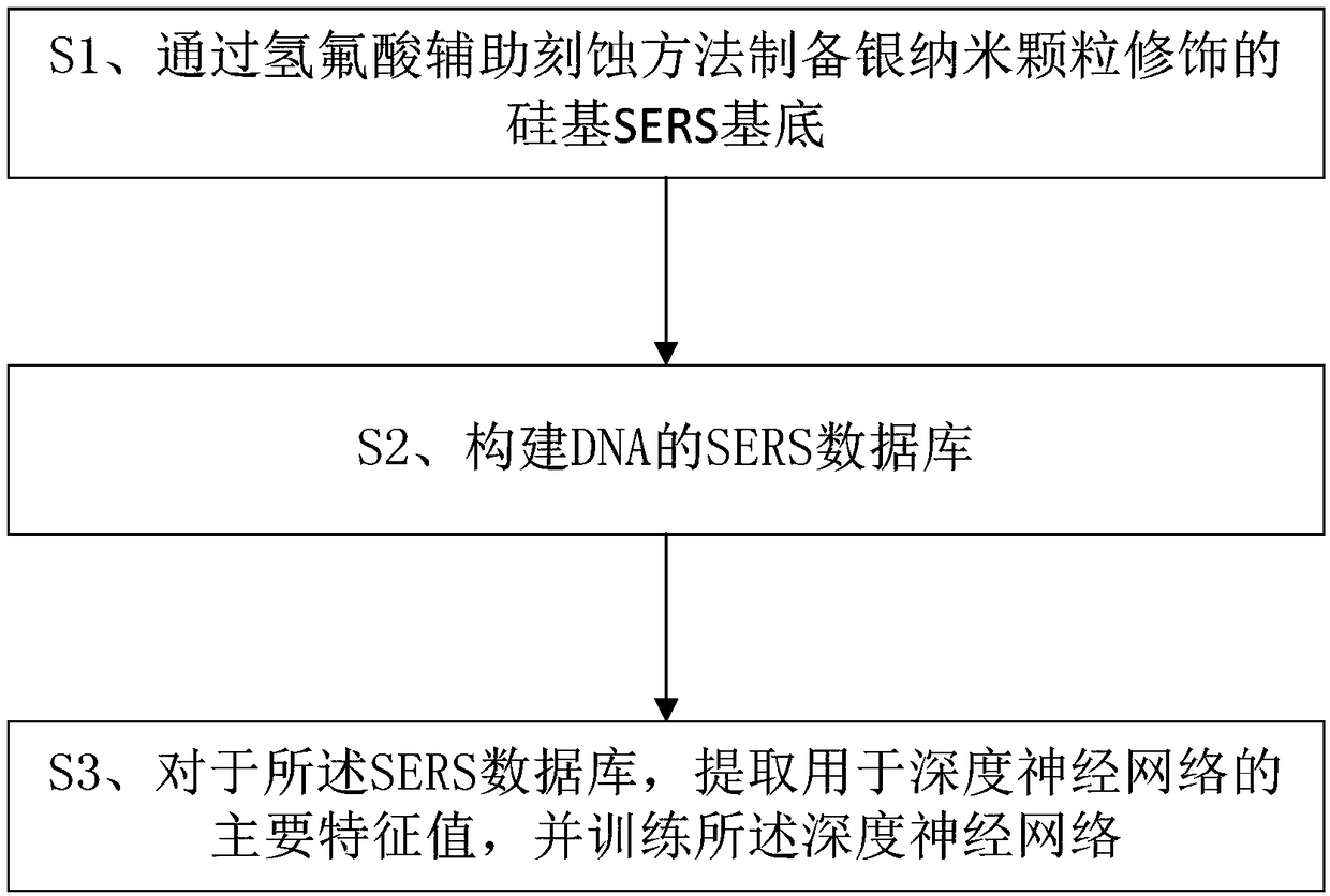
The invention discloses a silicon-based SERS chip DNA database constructing and training method used for artificial intelligence detection of DNA. The silicon-based SERS chip DNA database constructingand training method used for artificial intelligence detection of DNA comprises the following steps: preparing a silver nanoparticle modified silicon-based SERS substrate through a hydrofluoric acidassisted etching method; constructing a SERS database of DNA; and extracting main feature values used for a deep neural network for the SERS database, and training the deep neural network. The detection method disclosed by the invention can be carried out at room temperature; the operation is safe; the recognition rate of the DNA target can reach 86.11%; and the invention has good specificity, reproducibility and convenient detection process.

Description

technical field [0001] The invention belongs to the technical field of the combination of artificial intelligence and DNA detection, and specifically relates to a DNA sensing technology for building a database through a silicon-based SERS chip and applying it to a deep neural network. Background technique [0002] The deep belief network proposed in 2006 has become one of the breakthroughs in the history of artificial intelligence (AI) development (see: Nature 2015, 521, 436-444; Neural Comput. 2006, 18, 1527-1554). Since then, deep learning has made important progress in the development of many fields, such as autonomous driving, image recognition, speech recognition, machine translation, drug behavior prediction, gene mutation and disease prediction, etc. Even in the field of board games such as Go, deep learning plays an important role. For example, Google's deep learning software AlphaGo has defeated almost all human players in the game of Go (see: Nature 2016, 529, 484...

Claims


Application Information

Patent Timeline
Patent Type & Authority Applications(China)
IPC IPC(8): G06F19/18G06F19/28G06N3/04
CPCG06N3/045
Inventor 何耀王后禹史华意
Owner SUZHOU UNIV
Learn More