Photoelectric detector and manufacturing method thereof

A technology of photodetector and manufacturing method, which is applied in the field of photoelectric detection, can solve problems such as increasing product power consumption, unfavorable device photoresponsivity, and reducing, so as to improve photocurrent, meet the requirements of portability and multifunctionality, and improve The effect of photoresponsivity

Inactive Publication Date: 2018-12-14
SHANGHAI INTEGRATED CIRCUIT RES & DEV CENT
View PDF6 Cites 11 Cited by
  • Summary
  • Abstract
  • Description
  • Claims
  • Application Information

AI Technical Summary

Problems solved by technology

Especially in the field of photodetection, the existing photodetector needs to apply a high bias voltage between the two electrodes to separate the holes and electrons from the photosensitive material, which is not conducive to the improvement of the photoresponsivity of the device and the power consumption of the product. reduction of

Method used


Image

  • Photoelectric detector and manufacturing method thereof
  • Photoelectric detector and manufacturing method thereof
  • Photoelectric detector and manufacturing method thereof

Examples


Embodiment Construction

[0028] In order to make the purpose, advantages and characteristics of the present invention clearer, the following in conjunction with the attached Figure 1~5 The photodetector proposed by the present invention and its manufacturing method are further described in detail. It should be noted that all the drawings are in a very simplified form and use imprecise scales, and are only used to facilitate and clearly assist the purpose of illustrating the embodiments of the present invention.

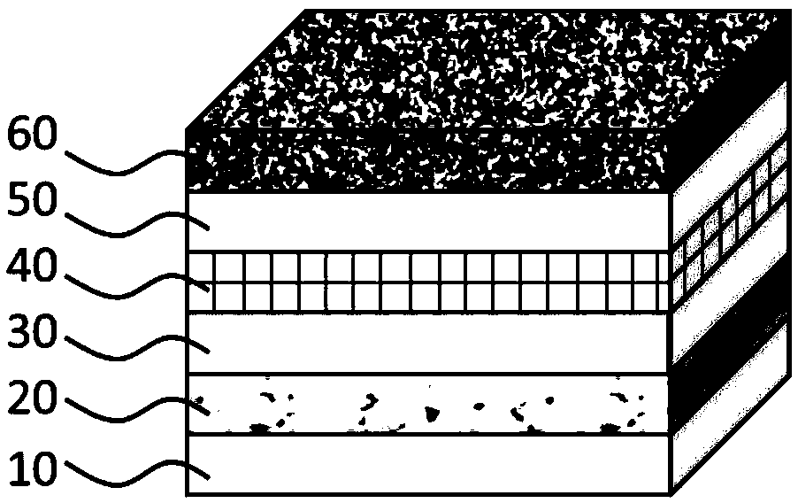
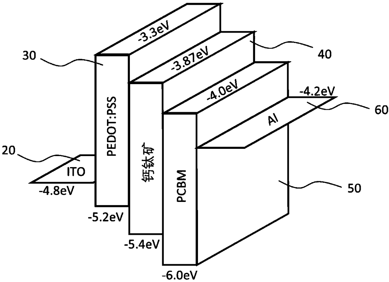
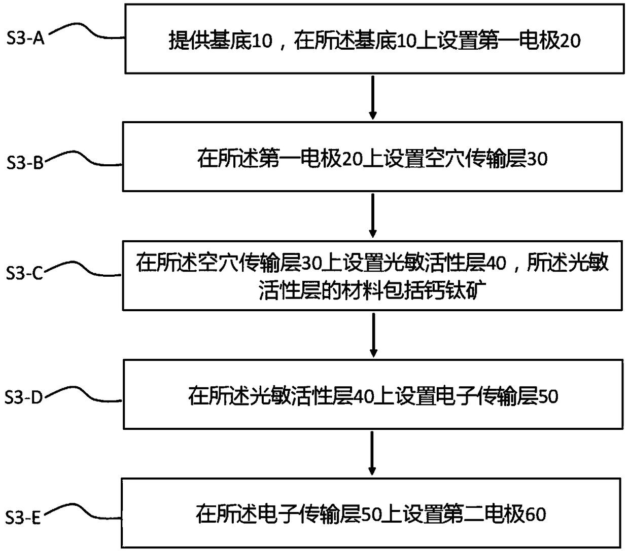
[0029] refer to figure 1 , figure 1 It is a structural schematic diagram of a photodetector provided by an embodiment of the present invention. The photodetector of this embodiment includes a substrate 10, a first electrode 20, a hole transport layer 30, a photosensitive active layer 40, an electron transport layer 50 and a second electrode 60, and the first electrode 20 is located on the substrate 10, The hole transport layer 30 is located on the first electrode 20, the photosensitive ac...


PUM


Abstract

The invention provides a photodetector and a manufacturing method thereof, wherein a photodetector with a vertical structure is manufactured by sequentially arranging a first electrode, a hole transport layer, a photosensitive active layer containing perovskite, an electron transport layer and a second electrode on a substrate from bottom to top. A PN junction is formed between the perovskite in the photosensitive active layer and the electron transport layer, thus the built-in electric field is constructed, thereby separating holes and electrons generated by the photosensitive active layer from each other only by applying a bias voltage of 0 V between the first electrode and the second electrode, The low driving voltage of the photodetector is realized, which is beneficial to the reduction of the power consumption of the product, and the hole transport layer and the electron transport layer are arranged above and below the photosensitive active layer respectively. The vertical arrangement mode can accelerate the transmission of holes and electrons, thereby increasing the photocurrent of the photodetector and further improving the photoresponsivity of the device. At that same time,each layer of the photodetector can be a flexible material to meet the requirements of portability and versatility.

Description

technical field [0001] The invention relates to the field of photoelectric detection, in particular to a photoelectric detector and a manufacturing method thereof. Background technique [0002] In recent years, photovoltaic devices based on organic-inorganic hybrid perovskites have attracted great attention due to their high energy conversion efficiency in the photovoltaic field. At the same time, because of the low exciton binding energy and high external quantum efficiency of perovskites , long carrier lifetime, and suppressed defect density make it of great potential value in optoelectronic fields such as photodetection and light-emitting diodes. Especially in the field of photodetection, the existing photodetector needs to apply a high bias voltage between the two electrodes to separate the holes and electrons from the photosensitive material, which is not conducive to the improvement of the photoresponsivity of the device and the power consumption of the product. decre...

Claims


Application Information

Patent Timeline
Patent Type & Authority Applications(China)
IPC IPC(8): H01L31/0352H01L31/18H01L31/101
CPCH01L31/035272H01L31/101H01L31/18Y02P70/50
Inventor 武青青朱建军胡少坚
Owner SHANGHAI INTEGRATED CIRCUIT RES & DEV CENT
Why Eureka
Try Eureka