Completely transparent microfluidic acoustic body wave chip and preparation method thereof

A microfluidic and acoustic technology, applied in the field of micro-total analysis system, can solve problems such as unfavorable observation and optical analysis and identification, increase the cost of preparation, limit the scope of application, etc., to achieve improved optical performance, improved visibility, and expanded applications range effect

Active Publication Date: 2018-12-18
WUHAN UNIV
View PDF4 Cites 10 Cited by
  • Summary
  • Abstract
  • Description
  • Claims
  • Application Information

AI Technical Summary

Problems solved by technology

This kind of acoustic wave chip has good airtightness, but it needs anodic bonding equipment worth millions, which increases the cost of preparation and limits its application range
Materials such as silicon waf

Method used


Image

  • Completely transparent microfluidic acoustic body wave chip and preparation method thereof
  • Completely transparent microfluidic acoustic body wave chip and preparation method thereof
  • Completely transparent microfluidic acoustic body wave chip and preparation method thereof

Examples


Embodiment 1

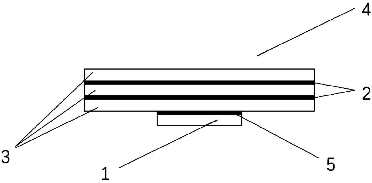
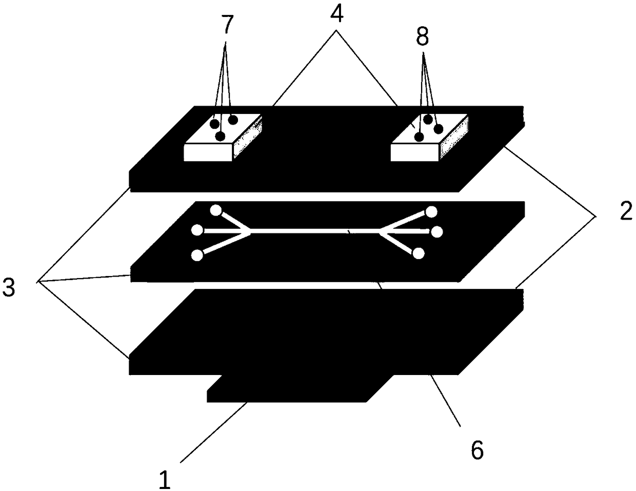
[0041] Fabrication of fully transparent microfluidic volume wave chip

[0042] The preparation steps are as follows:

[0043] 1) Cutting three glass sheets 3 with the same size and a thickness of 300-500 microns, the upper glass sheet is opened with a sample inlet 7 and a sample outlet 8 for fluid inlet and outlet, and the number of inlet and outlet samples is 3; The middle glass sheet is cut with a micron-level channel 6 through the glass cut by laser, and the three sample inlets 7 are converged to the central channel and then divided into three sample outlets 8; the lower glass sheet is complete glass for packaging chamber;

[0044] 2) Evenly spin-coat the UV-curable epoxy resin layer 2 on the uppermost and lowermost glass surfaces through a glue leveler, and then paste them on the two sides of the middle glass respectively to ensure that the hole positions of the inlet and outlet of the upper glass and the middle glass are aligned , bonded by ultraviolet light irradiation...

Embodiment 2

[0050] The application effect contrast of embodiment 1 and comparative example 1

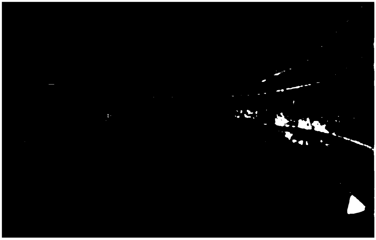
[0051] attached image 3 It is the application effect diagram of Comparative Example 1. Depend on image 3 It can be seen that the 15 μm polystyrene microspheres are obviously gathered into two lines in the channel, which can achieve the effect of particle aggregation and manipulation.

[0052] attached Figure 4It is the application effect diagram of embodiment 1. In the figure, the 15 μm silica microspheres are brought together in the channel to the two parallel lines in the middle area under the action of the sound field.

[0053] From attached image 3 And attached Figure 4 It can be seen that the chip prepared by the present invention has the same effect as the prior art product in actual use.


PUM

PropertyMeasurementUnit
Thicknessaaaaaaaaaa
Thicknessaaaaaaaaaa

Abstract

The invention discloses a completely transparent microfluidic acoustic body wave chip and a preparation method thereof. The product consists of three glass sheets and one piece of piezoelectric material. The three glass sheets are stacked from top to bottom to form a standing wave reaction chamber, the upper glass sheet is equipped with holes for fluid to come in and out by laser, and thick piecesof polydimethylsiloxane (PDMS) with corresponding holes are bonded to the surface holes. A micron-scale channel is prepared on the middle glass sheet by laser cutting and penetration of the glass. The lower glass is complete glass, and is used for chamber encapsulation. The piezoelectric material is made of lithium niobate single crystal, the upper surface and lower surface of the piezoelectric material are both plated with a layer of transparent tin-doped indium oxide (ITO) conductive film, and the piezoelectric material is sticked at the lower surface of a resonant cavity, both sides of thelithium niobate wafer undergo silver slurry curing, and two leads are led out. The chip prepared by the method provided by the invention is completely transparent and highly visible, and can be usedfor gathering, separation and manipulation of cells/particles and other samples. The preparation process adopted by the invention is simple, and the cost is low.

Description

technical field [0001] The invention belongs to the field of micro total analysis systems, in particular to a fully transparent microfluidic acoustic body wave chip and a preparation method thereof. Background technique [0002] Due to the rapid development of micro-electro-mechanical processing technology (MicroElectrical-Mechanical System, MEMS), research on microfluidic technology has also begun to receive widespread attention. In the last three decades, microfluidic chips based on microfabrication have shown promising application prospects in the fields of physics, chemistry, and biology. Due to its miniaturization and easy integration, the microfluidic chip makes it possible to complete various functions of sample detection, control and analysis on a coin-sized chip. Due to its small size, high sensitivity, high biocompatibility, high integration, non-contact and other advantages, the acoustic microfluidic chip has attracted extensive attention and has become one of th...

Claims


Application Information

Patent Timeline
IPC IPC(8): B01L3/00
CPCB01L3/5027B01L2200/10B01L2300/0861B01L2300/0887B01L2300/12
Inventor 国世上舒溪吴泽政
Owner WUHAN UNIV
Why Eureka
Try Eureka