Flip-chip structure micro-size photonic crystal LED array chip and preparation method thereof

An LED array and photonic crystal technology, which is applied in the field of flip-chip micro-size photonic crystal LED array chips and their preparation, can solve problems such as poor ohmic contact performance, and achieve improved recombination rate, improved luminous efficiency and modulation bandwidth, and improved output. The effect of optical power

Pending Publication Date: 2019-01-15
SOUTH CHINA UNIV OF TECH
View PDF0 Cites 12 Cited by
  • Summary
  • Abstract
  • Description
  • Claims
  • Application Information

AI Technical Summary

Problems solved by technology

Difficulty 3 is the preparation of the ohmic contact layer: when the ohmic contact layer is prepared on the surface of the photonic crystal, the contact area between the ohmic contact layer and the semiconductor material is small, so the ohmic contact performance is poor

Method used


Image

  • Flip-chip structure micro-size photonic crystal LED array chip and preparation method thereof
  • Flip-chip structure micro-size photonic crystal LED array chip and preparation method thereof
  • Flip-chip structure micro-size photonic crystal LED array chip and preparation method thereof

Examples


Embodiment 1

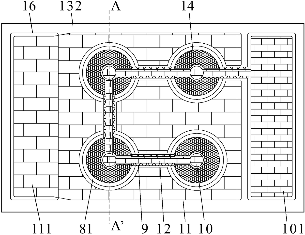
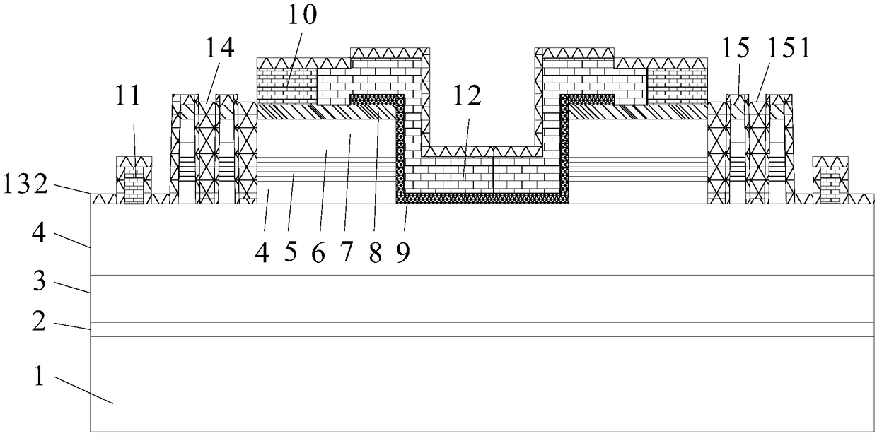
[0052] Embodiment 1, the preparation steps of the flip-chip micro-sized photonic crystal LED array chip are as follows.

[0053] (1) GaN-based LED epitaxial wafers are prepared by metal oxide vapor deposition. The structure of GaN-based LED epitaxial wafers includes sapphire substrate 1, GaN buffer layer 2, unintentionally doped GaN layer 3, and N-type doped GaN layer. 4. Quantum well layer 5 , P-type doped AlGaN layer 6 and P-type doped GaN layer 7 .

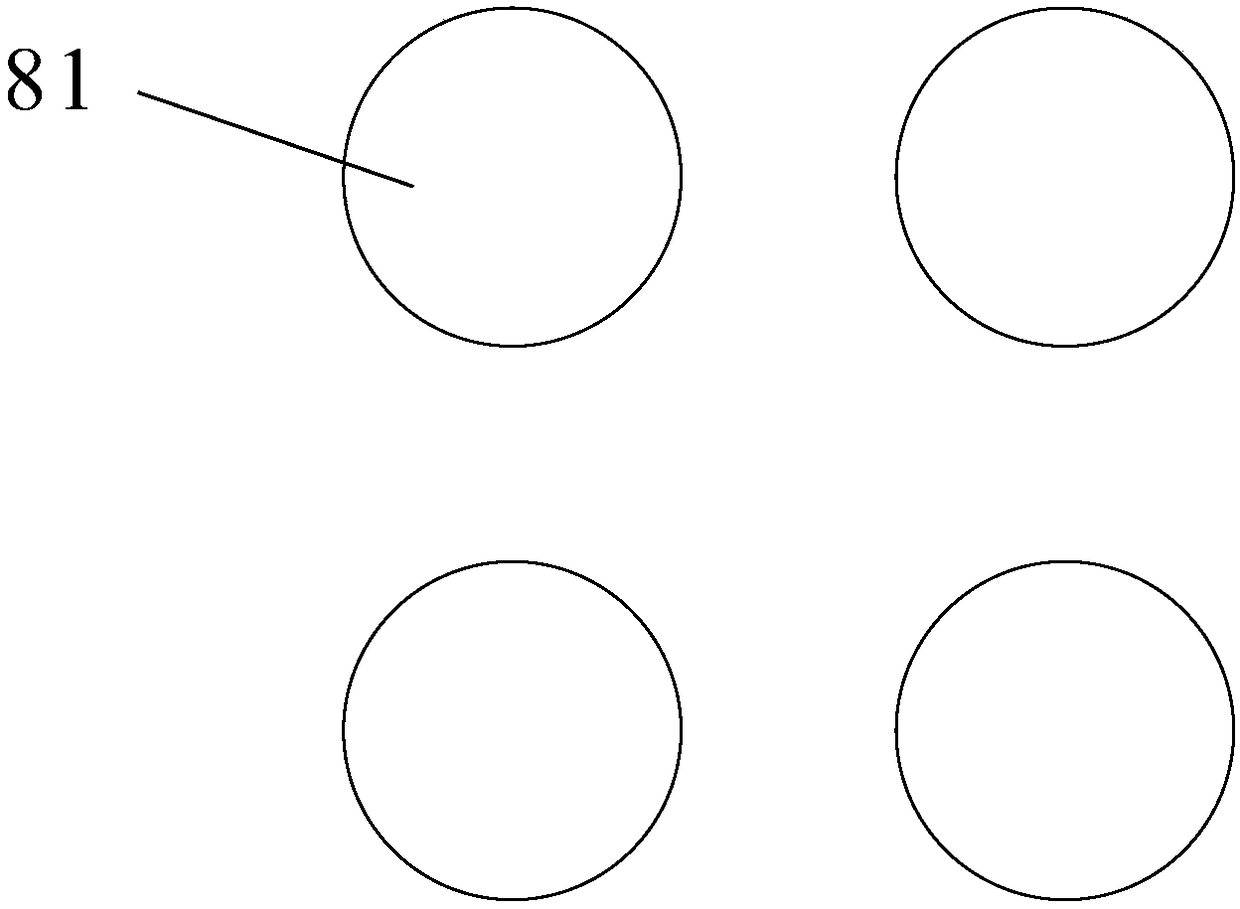
[0054] (2) Deposit a transparent current spreading layer ITO 8 with a thickness of 100 nm on the GaN-based LED epitaxial wafer using electron beam evaporation, in N 2 200sccm, O 2 Rapid annealing in a mixed atmosphere of 35 sccm for 3 minutes to form an ohmic contact, and then use ultraviolet lithography and wet etching, and soak in ITO etching solution for 15 minutes at room temperature to form an ITO disc 8 distributed only in the active area of ​​the light-emitting unit. 98 μm in diameter.

[0055] (3) Etching by induct...


PUM


Abstract

The invention discloses a flip-chip structure micro-size photonic crystal LED array chip and a preparation method thereof. The LED array chip of the invention has four light emitting units connected in parallel, the metal connecting line of the positive electrode and the semiconductor material are separated by a dielectric insulation layer, and the negative electrode is directly covered on the upper surface of the semiconductor material. The active region of the light-emitting unit has a photonic crystal with periodic distribution, and the depth of the photonic crystal exceeds the depth of theactive layer. Except electrode pad, DBR is distributed on the whole chip surface. Metal electrodes form metal mirrors. The preparation method of the invention adopts the scheme that an ohmic contactlayer and an electrode are firstly prepared and then a photonic crystal is etched without planarizing and the like traditional process flow; Using thick strip dielectric insulating layer to insulate the electrode from semiconductor material and thin dielectric mask layer and adhesive mask layer to etch together is conducive to the deposition of DBR and the rapid escape of photon mode. The processflow of the invention is simple and reliable.

Description

technical field [0001] The invention relates to the field of photonic crystal LED chips, in particular to a flip-chip micro-sized photonic crystal LED array chip and a preparation method thereof. Background technique [0002] Visible light communication takes into account both lighting and communication functions, and has become an important breakthrough point for LEDs (light-emitting diodes) in the field of lighting. In visible light communication, the modulation bandwidth of light-emitting devices is an important factor affecting the communication capacity. The modulation bandwidth of LED is mainly affected by RC constant and carrier recombination rate. In order to reduce the RC constant to increase the RC bandwidth, micro-sized chips can be used; in order to increase the carrier recombination rate to increase the carrier confinement bandwidth, resonant cavity, surface plasmon and photonic crystal technology can be used. [0003] The micro-sized chip not only has a small...

Claims


Application Information

Patent Timeline
Patent Type & Authority Applications(China)
IPC IPC(8): H01L27/15H01L33/14H01L33/10H01L33/46H01L33/00
CPCH01L27/15H01L33/007H01L33/10H01L33/14H01L33/46
Inventor 黄华茂黄程吴浩城王洪
Owner SOUTH CHINA UNIV OF TECH
Why Eureka
Try Eureka