

A method for manufacturing a flexible color micro-LED display device
A display device and flexible technology, applied in the field of flexible color micro-LED display device preparation, can solve the problems of low color rendering index, narrow phosphor excitation band, low conversion efficiency, etc., achieve high pixel density, fast and effective manufacturing method, low cost effect
- Summary
- Abstract
- Description
- Claims
- Application Information
AI Technical Summary
Problems solved by technology
Method used
Image

Examples
preparation example Construction
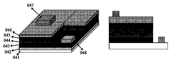
[0030] The preparation method of the flexible color filter film comprises the following steps:
[0031] Step S01: Prepare quantum dot polymer solutions with different luminescent wavelengths respectively;
[0032] Step S02: preparing a liquid polymer resin as the main body of the flexible color filter film;
[0033] Step S03: Use inkjet printing to print quantum dot polymer solutions with different luminous wavelengths on the liquid polymer resin according to the corresponding micro-LED array arrangement, and use the liquid polymer resin to suppress the diffusion of the quantum dot polymer solution , to prepare a high-density quantum dot lattice;
[0034] Step S04: Control the standing time of the quantum dots on the liquid polymer resin, so that the quantum dots completely sink into the liquid polymer resin, by controlling the viscosity of the glue in the liquid polymer resin, the size of the inkjet printing nozzle, and the ink droplet The pressure and the number of ink dro...
specific Embodiment 1
[0082] Include the following steps:
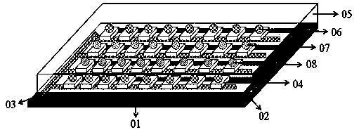
[0083] (1) Take a clean flexible substrate, and determine the area and pattern of the electrode on the flexible substrate by photolithography and wet etching. The size of the electrode is 4500 μm × 20 μm;
[0084] (2) Apply an adhesive on the determined area to promote the bonding between the flexible substrate and the metal electrode, and then use an electron gun to coat 10g of metal copper into the established area with a thickness of about 25 μm;
[0085] (3) Prepare the sapphire substrate and perform patterning on its surface. The pattern is cone-shaped, the diameter of each pattern is 2.1 μm, the height is 1.3 μm, and the interval between patterns is 900 nm;
[0086] (4) A 2μm undoped GaN buffer layer, a 3μm silicon-doped n-GaN, and a 100nm InGaN / GaN active layer (MQW) with a center wavelength of 380nm were grown on sapphire by metal organic chemical vapor deposition (MOCVD) and 0.2 μm magnesium-doped p-GaN;
[0087] (5) Prepare a l...
specific Embodiment 2
[0095] Include the following steps:
[0096] (1) Take a flexible TFT panel or a flexible CMOS panel;
[0097] (2) Bonding the prepared micro-LED array to the above driving panel;
[0098] (3) Prepare PDMS glue, and apply it to the fabricated flexible micro-LED device by scraping;
[0099] (4) Preparation of quantum dot polymer solution;
[0100] (5) Use the inkjet printing method to hit the prepared quantum dot polymer solution on the surface of PDMS, let it stand for 5-15 minutes, and then heat it at 80°C for 3 hours to volatilize the organic solvent in the solution and cure the PDMS film layer.
[0101] Parts similar to those in Embodiment 1 will not be repeated here.
PUM
 Abstract
Description
Claims
Application Information