
A nanometer bimetallic layer back contact for undoped heterogeneous n-type single polished silicon solar cell and preparation method and application thereof are disclosed

A technology of silicon solar cells and double metal layers, which is applied in the field of solar cell technology, can solve the problems of poor repeatability, unsuitability for non-doped heterogeneous n-type single-throw silicon solar cells, and increase the complexity of the preparation process, achieving a balanced preparation Process and product performance, facilitate extraction and transport, improve energy conversion efficiency effects

Inactive Publication Date: 2019-01-22
JINAN UNIVERSITY
View PDF5 Cites 2 Cited by
  • Summary
  • Abstract
  • Description
  • Claims
  • Application Information

AI Technical Summary

Problems solved by technology

[0003] In traditional crystalline silicon solar cells, the back contact is mostly prepared by high-temperature doping, but this preparation method leads to an increase in the cost of the solar cell, and is not suitable for low-cost non-doped heterogeneous n-type single-throw silicon solar cells
Liquid Ga / In alloy electrodes are limited by the preparation process and have poor repeatability
In the solution method to prepare the back contact, it is necessary to seal the edges around the battery, which increases the complexity of the preparation process.
If Al or Ag is directly used as the back electrode, it cannot form ohmic contact with silicon, and the contact resistance is large, resulting in low energy conversion efficiency of the solar cell.
[0004] At present, methods to improve the energy conversion efficiency of non-doped heterogeneous n-type single-throw silicon solar cells have been reported in the literature, including structuring the front side of crystalline silicon, improving the contact between organic layers and silicon, and optimizing hole-selective contacts. The optimization of the back contact, but the optimization of the back contact still needs to be further improved and enhanced in terms of preparation process, preparation cost and battery energy conversion efficiency

Method used


Image

  • A nanometer bimetallic layer back contact for undoped heterogeneous n-type single polished silicon solar cell and preparation method and application thereof are disclosed
  • A nanometer bimetallic layer back contact for undoped heterogeneous n-type single polished silicon solar cell and preparation method and application thereof are disclosed

Examples


Embodiment 1

[0031] Example 1 Preparation of nano-double metal layer back contact non-doped heterogeneous n-type single-throw silicon solar cell

[0032] Taking the back contact of Ag0.5Mg10 nanometer double metal layer as an example, Ag is a nanometer ultra-thin metal adhesion layer with a thickness of 0.5nm; Mg is an electron selective transport nanometer metal layer with a thickness of 10nm; the specific preparation process And the specific process of preparing non-doped heterogeneous n-type single-throw silicon solar cells is as follows:

[0033] (1) Soak a clean n-type single-sided polished silicon wafer (resistivity 0.05-0.1 Ω cm) in a hydrofluoric acid solution with a concentration of 10 M for 5 min to remove silicon oxide, and dry it;

[0034] (2) Coat the polished surface of the above-mentioned silicon wafer with an organic layer of PEDOT:PSS (PH1000), and anneal at 140°C for 10 minutes;

[0035] (3) Move the silicon wafer coated with the organic layer in step (2) to the vacuum c...

Embodiment 2

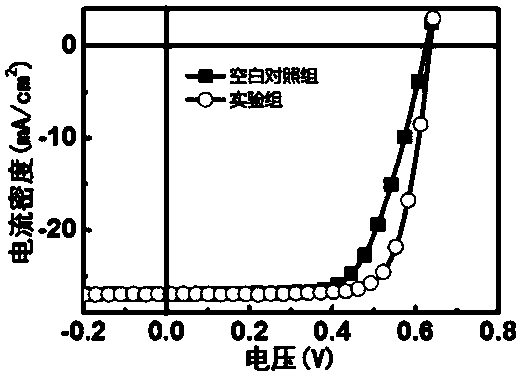
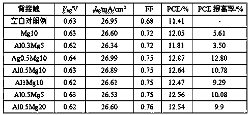
[0039] With reference to the preparation method in Example 1, the difference is to change the metal type of the nano-ultra-thin metal adhesion layer, applicable metals are Al, Ag and Au; change the thickness of the nano-ultra-thin metal adhesion layer, or electron selective transmission The thickness of the nano-metal magnesium layer, here are several representative back contacts, including Al0.5Mg10 nanometer double metal layer back contact, Al0.5Mg5 nanometer double metal layer back contact, Al0.5Mg20 nanometer double metal layer back contact and Au0.5Mg10 nanometer bimetallic layer back contact.

[0040] The representative nano-double metal layer back contact prepared above was prepared into a non-doped heterogeneous n-type single-throw silicon solar cell according to the method described in Example 1, and its energy conversion (PCE )performance.

[0041] Among them, the n-type single-polished silicon without nano-ultra-thin metal adhesion layer and electron selective tran...


PUM

PropertyMeasurementUnit
thicknessaaaaaaaaaa
thicknessaaaaaaaaaa
thicknessaaaaaaaaaa

Abstract

The invention discloses a nanometer bimetallic layer back contact for undoped heterogeneous n-type single parabolic silicon solar cell and a preparation method and application thereof. The back contact is a nanometer ultra-thin metal adhesion layer and an electron selective transmission nanometer metal layer which are sequentially plated on the back surface of the n-type single-thrown silicon; Thenanometer ultra-thin metal adhesion layer is aluminum, silver or gold, and the thickness thereof is 0.5 to 1 nm; The electron selective transmission nanometer metal layer is magnesium, and the thickness thereof is 5-20 nm. The nano bimetallic layer provided by the invention selectively transmits electrons in the back contact of the nano bimetallic layer and the contact and adhesion between the nano metallic layer and the silicon are better, the work function of the metal electrode can be reduced, the transmission of electrons from the silicon to the electrode is more favorable, and the energyconversion efficiency of the undoped heterogeneous n-type single parabolic silicon solar cell is further improved. Moreover, the preparation process of the nano bimetallic layer back contact is simple, no annealing process is required, the cost is low, the preparation process and the product performance are taken into consideration, and the nano bimetallic layer back contact is suitable for large-scale industrial production.

Description

technical field [0001] The invention belongs to the technical field of solar cell technology, and in particular relates to a nanometer double metal layer back contact for a non-doped heterogeneous n-type single-throw silicon solar cell, and a preparation method and application thereof. Background technique [0002] Dopant-Free Heterojunction Solar Cells based on n-type one side polished Sillicon (Dopant-Free Heterojunction Solar Cells based on n-type one side polished Sillicon) does not require high-temperature doping during its preparation, and organic polymers and crystalline silicon are formed by solution processing The p-n heterojunction replaces the traditional diffusion process, which greatly reduces the cost of heterogeneous crystalline silicon solar cells. It has potential application prospects and is developing rapidly. [0003] In traditional crystalline silicon solar cells, the back contact is mostly prepared by high-temperature doping, but this preparation method...

Claims


Application Information

Patent Timeline
Patent Type & Authority Applications(China)
IPC IPC(8): H01L31/0224H01L31/042
CPCH01L31/022441H01L31/042Y02E10/50
Inventor 杨玉照麦耀华吕晓宁
Owner JINAN UNIVERSITY
Learn More