Phase-change-controllable totally-inorganic perovskite thin film preparation method and device application

A technology for film preparation and inorganic calcium, which is applied in the field of all-inorganic perovskite film preparation to achieve simple process conditions, reduce defect state density, and improve crystal quality

Active Publication Date: 2019-02-19
CHANGZHOU INST OF TECH
View PDF0 Cites 14 Cited by
  • Summary
  • Abstract
  • Description
  • Claims
  • Application Information

AI Technical Summary

Problems solved by technology

However, for the industrial application of large-scale perovskite devices, the solution method will be limited by insuff

Method used


Image

  • Phase-change-controllable totally-inorganic perovskite thin film preparation method and device application
  • Phase-change-controllable totally-inorganic perovskite thin film preparation method and device application
  • Phase-change-controllable totally-inorganic perovskite thin film preparation method and device application

Examples


Embodiment 1

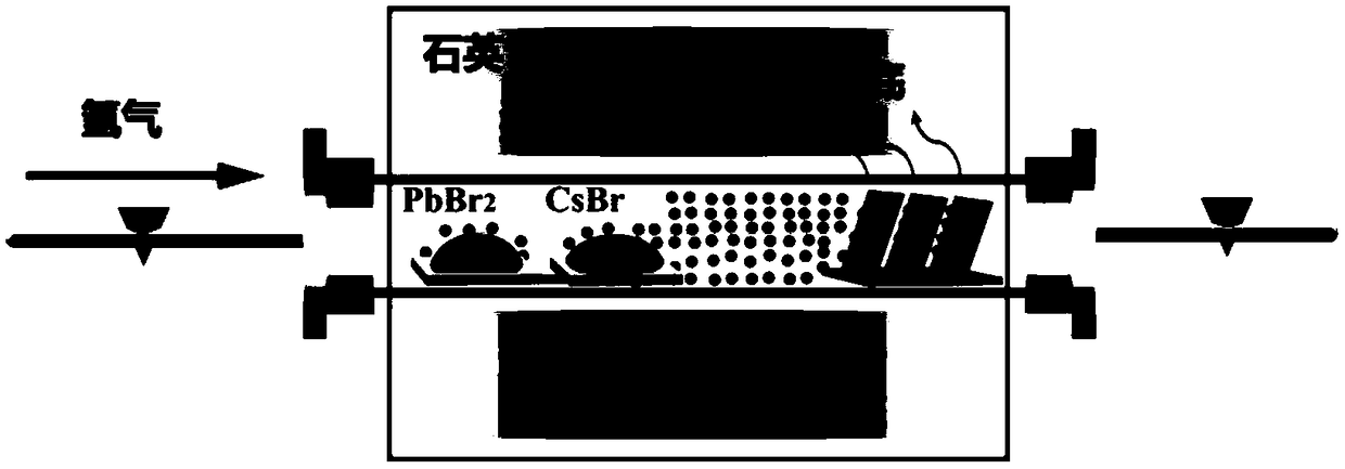
[0032] The vapor deposition device used in this example and the principle of preparing perovskite film by chemical vapor deposition are as follows figure 1 shown. All adopt chemical vapor deposition (CVD) device in the embodiment, and reactant is cesium bromide and lead bromide, and purity is all more than 99%, and carrier gas is argon, and purity is more than 99%, and substrate material selects silicon for use, P type, (100) crystal plane. In the device fabrication process, interdigitated electrodes are used as the substrate, and the electrode material is gold. All are commercially available products.

[0033] Growth of CsPb by CVD Technique 2 Br 5 Perovskite thin film materials:

[0034] 1. The reactant cesium bromide and lead bromide are respectively placed in the CVD system, and the substrate is placed in the deposition area, which is conducive to the reaction and deposition of gas phase substances;

[0035] 2. Start the mechanical pump, evacuate to 100Pa, repeat thr...

Embodiment 2

[0042] The vapor deposition device and raw materials of this embodiment are the same as those of Embodiment 1.

[0043] Growth of CsPb by CVD Technique 2 Br 5 -CsPbBr 3 Dual-phase perovskite thin film materials

[0044] Preparation steps and processing conditions are as described in Example 1, the difference is:

[0045] Process conditions: the growth temperature is 600° C., the heating time from room temperature to 600° C. is 60 minutes, the reaction time at this temperature is 40 minutes, and the flow rate of the carrier gas is 80 sccm.

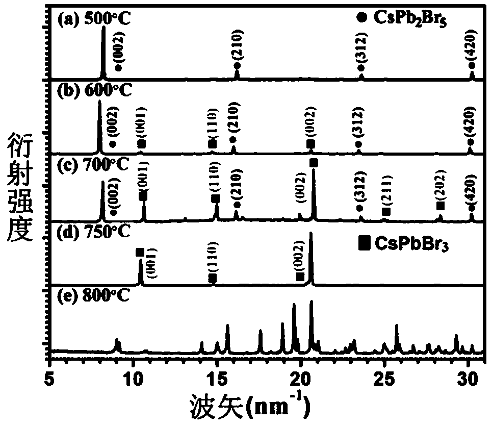
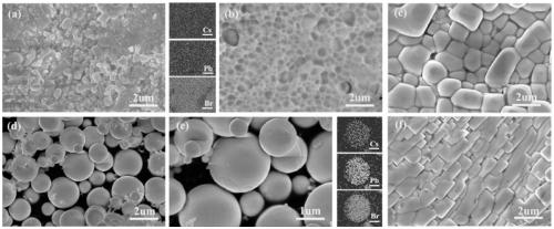
[0046] Such as figure 2 As shown in b, the perovskite prepared at 600°C is CsPb 2 Br 5 -CsPbBr 3 Dual-phase structure, that is, CsPbBr starts to appear in the perovskite 3 Mutually. Such as image 3b It is known that the surface of the perovskite film is relatively uniform and the particle size increases

[0047] Deposit the above perovskite thin film on the interdigitated electrodes of the silicon substrate, and the electrode m...

Embodiment 3

[0049] The vapor deposition device and raw materials of this embodiment are the same as those of Embodiment 1.

[0050] Growth of CsPb2Br5-CsPbBr3 Dual Phase Perovskite Thin Films by CVD

[0051] Preparation steps and processing conditions are as described in Example 1, the difference is:

[0052] Process conditions: the growth temperature is 700° C., the heating time from room temperature to 700° C. is 60 minutes, the reaction time at this temperature is 40 minutes, and the flow rate of the carrier gas is 80 sccm.

[0053] Such as figure 2 As shown in c, the perovskite prepared at 700°C is CsPb 2 Br 5 -CsPbBr 3 Duplex structure, CsPbBr 3 Significantly increased relative gravity. Such as image 3 It can be seen from c that the particle size on the surface of the perovskite film is relatively large.

[0054] Deposit the above perovskite thin film on the interdigitated electrodes of the silicon substrate, and the electrode material is gold to obtain a perovskite photoel...


PUM


Abstract

The invention belongs to the technical field of photoelectric functional materials and particularly relates to a phase-change-controllable totally-inorganic perovskite thin film preparation method anddevice application. The method comprises the steps that (1), precursor lead bromide and cesium bromide are placed into a vapor deposition device correspondingly, a substrate is placed in a depositionarea, and vacuum pumping is performed on the whole device; (2), an inert gas is introduced into the vapor deposition device; (3), the deposition temperature and deposition time are set, the deposition temperature is selected from 500-800 DEG C, and at the different deposition temperature, perovskite thin film has different composition and crystal forms. The phase-change-controllable totally-inorganic perovskite thin film preparation method and the device application adopt a chemical vapor deposition method, are simple in process condition, easy to control accurately and suitable for industrial production; meanwhile, the thin film has good uniformity and has good adhesiveness and spreadability with the substrate material, and the prepared optoelectronic thin film has broad application prospects; and by means of change of the deposition temperature, controllable growth of perovskite phase from CsPb2Br5 to CsPbBr3 is realized, and a photoelectric detector prepared on base of the perovskite thin film obtained by the phase-change-controllable totally-inorganic perovskite thin film preparation method shows good photoelectric response and switching characteristics.

Description

technical field [0001] The invention belongs to the technical field of photoelectric functional materials, and in particular relates to a preparation method and device application of an all-inorganic perovskite thin film with controllable phase change. Background technique [0002] In recent years, organic-inorganic hybrid perovskites have great application prospects in the fields of solar cells, light-emitting diodes, and detectors due to their broad-spectrum absorption, adjustable electronic properties, and high carrier mobility. However, the phenomena of phase separation and light-induced halogen separation largely hinder the development of organic-inorganic hybrid perovskite materials. The use of metal ions (such as cesium, rubidium, etc.) instead of organic ions is a very good solution to the thermal instability of perovskites. Therefore, a variety of solution-based methods have been used to grow morphology-controlled all-inorganic perovskite crystals, and perovskite d...

Claims


Application Information

Patent Timeline
IPC IPC(8): C23C16/30C23C16/52H01L31/032H01L31/09H01L31/18
CPCC23C16/30C23C16/52H01L31/032H01L31/09H01L31/18Y02P70/50
Inventor 徐伟龙蔡小红陈海悦郑敏肖进赵宇卞维柏
Owner CHANGZHOU INST OF TECH
Why Eureka
Try Eureka