Semiconductor device

A semiconductor and N-type semiconductor technology, applied in semiconductor devices, electrical components, diodes, etc., can solve problems such as gate runaway, oxide layer breakdown, failure, etc.

Active Publication Date: 2019-03-05
NANJING SINNOPOWER TECH CO LTD
View PDF5 Cites 11 Cited by
  • Summary
  • Abstract
  • Description
  • Claims
  • Application Information

AI Technical Summary

Problems solved by technology

The failure mechanism can be roughly attributed to the following aspects: 1) Failure caused by parasitic thyristor latch-up (Latch-up); 2) Failure caused by device self-heating under high voltage and high current exceeding the maximum junction temperature; 3 ) due to gate-collector capacitance (C GC ), the g

Method used


Image

  • Semiconductor device
  • Semiconductor device
  • Semiconductor device

Examples


Embodiment 1

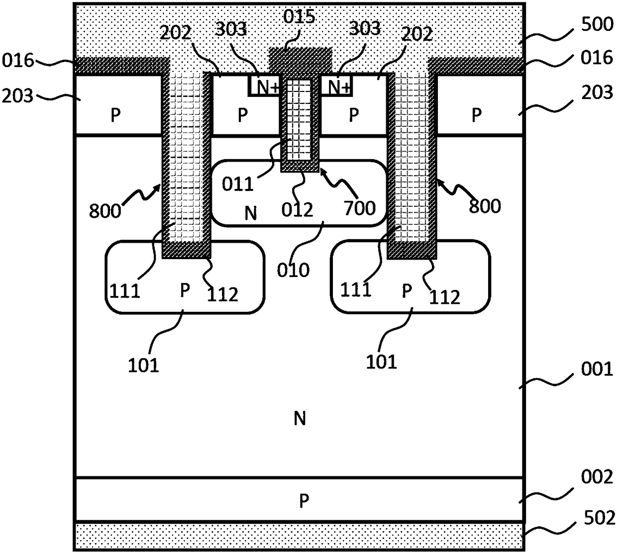
[0056] The MOS-controlled bipolar transistor (MCBT) proposed by the present invention is composed of a plurality of cell units, figure 1A schematic diagram of the cross-sectional structure of one of the cells. The cellular structure uses an N-type substrate 001 as a substrate, a P-type semiconductor region 002, called an anode region, is provided on one side of the N-substrate 001, and at least one first tank unit 700 and At least one second tank unit 800 , wherein the depth of the first tank unit 700 is smaller than that of the second tank unit 800 . At the bottom of the first tank unit 700, there is an N-type carrier barrier region 010 with a higher doping concentration than the N substrate 001, which is called a minority carrier barrier region, and a P-type electric field is provided at the bottom of the second tank unit 800 Shielded area 101. A gate region 011 is provided in the first cell unit 700, and a first medium 012 is provided between the gate region 011 and the N...

Embodiment 2

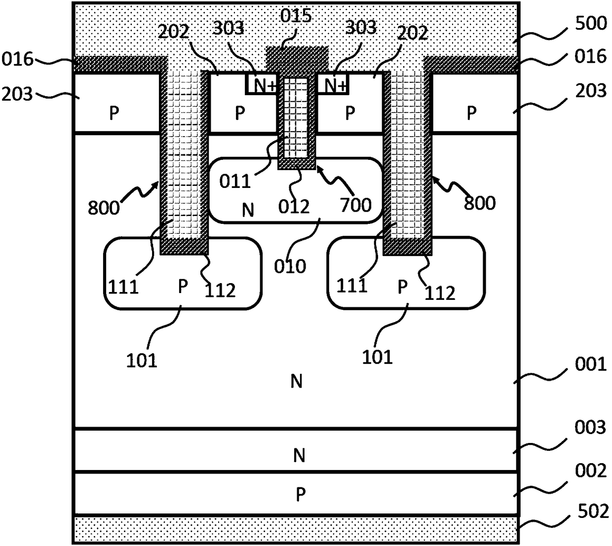
[0069] In the above embodiments, the N-type substrate 001 is non-punch-through, that is, the N-type substrate region 001 will not be fully depleted when the highest voltage is applied between the collector and the emitter. Embodiment 2 provides a PunchThrough or Field Stop cell, the schematic diagram of which is shown in figure 2 shown. There is a first N-type semiconductor region 003 adjacent to the P-type semiconductor region 002 , which is called a field stop region, and the doping concentration of the field stop region 003 is higher than that of the N-type substrate 001 . As the name implies, when the highest voltage is applied between the collector and the emitter, the electric field is cut off in the field stop region 003, and the field stop region 003 will not be completely depleted. The electric field stop structure in Example 2 can obtain a smaller thickness of the N-type substrate 001 than in Example 1.

[0070] Since the thickness of the N-type substrate 001 is r...

Embodiment 3

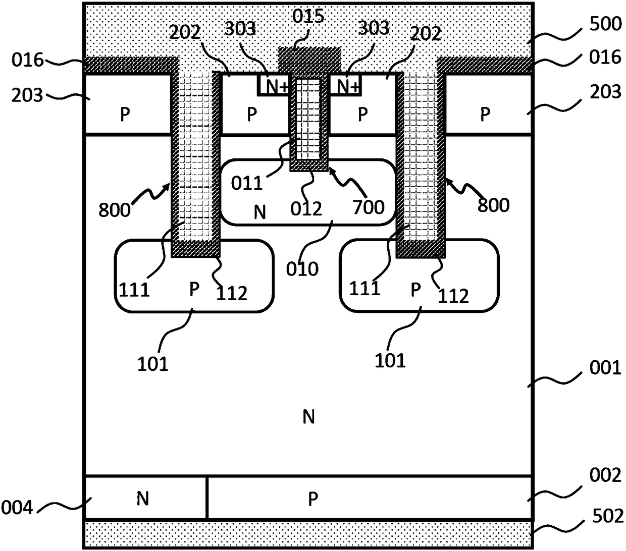
[0072] Embodiment 3 provides a cell of reverse conduction type (Reverse Conduction), and its structural schematic diagram is as follows image 3 shown. There is a second N-type semiconductor region 004 on the side adjacent to the P-type semiconductor region 002, and both the P-type semiconductor region 002 and the second N-type semiconductor region 004 are in direct contact with the first electrode 502, forming an anode short circuit (Anode Short) structure .

[0073] A P-N-N diode is formed by the P-type source-body region 202, the N-type carrier barrier region 010, the N-type substrate 001, and the second N-type semiconductor region 004. When the potential of the emitter second electrode 500 is higher than that of the collector first electrode When the potential of the electrode 502 is constant, the P-N-N diode is forward-biased, and at this time, a current flows from the emitter second electrode 500 to the collector first electrode 502 to form a reverse conduction.

[007...


PUM


Abstract

Disclosed is a semiconductor device. The semiconductor device comprises at least one cell, and the structure of any cell comprises an N-type substrate, at least one N-type carrier barrier region, andat least one P-type electric field shielding region, wherein at least one first groove unit and at least one second groove unit are included on one side of the N-type substrate; at least one P-type semiconductor region is arranged on the other side of the N-type substrate, wherein the P-type semiconductor region is referred to as an anode region. The invention aims to provide the semiconductor device, wherein the semiconductor device has a novel cellular structure so as to obtain a large safe operating area, and the anti-short-circuit capability; the effect of a parasitic thyristor is eliminated; the low-grid-collector charges (QGC) are adopted to obtain the maximum anti-dv/dt capability; the emitter side electric conduction modulation is added, so that a relatively large current density and an extremely low conducting voltage drop can be obtained; and relatively turn-off loss and relatively low process complexity are achieved.

Description

technical field [0001] The invention relates to the technical field of semiconductors, in particular to a semiconductor device. Background technique [0002] As we all know, an insulated gate bipolar transistor (Insulated Gate Bipolar Transistor, referred to as IGBT) is a composite full-control voltage-driven power semiconductor device composed of an insulated gate field effect transistor (MOS) and a bipolar transistor (BJT). High input impedance, low driving power, simple driving circuit, fast switching speed and low conduction voltage, etc., are extremely useful in the fields of household appliances, rail transit, smart grid, aerospace, electric vehicles and new energy equipment. It is widely used and is the core device of electric energy conversion and transmission. [0003] As the core device of power electronics technology, the IGBT must not only work in the rated state, but also withstand the extreme conditions that often occur in the power system, such as overvoltage...

Claims


Application Information

Patent Timeline
IPC IPC(8): H01L29/06H01L29/739
CPCH01L29/0607H01L29/0657H01L29/7393H01L29/0619H01L29/0623H01L29/0834H01L29/407H01L29/7397H01L29/744H01L29/861H01L29/87H01L29/1095H01L29/4236H01L29/7395H01L29/7412
Inventor 吕信江
Owner NANJING SINNOPOWER TECH CO LTD
Why Eureka
Try Eureka