Infrared light detection thin film, device and display device and fabrication method of infrared light sensing thin film

A display device and infrared light technology, applied in the field of optical devices, can solve the problems of easy pollution, high cost, complicated process, etc., and achieve the effect of reducing the probability of recombination and increasing excitation

Active Publication Date: 2019-03-05
SHANGHAI HARVEST INTELLIGENCE TECH CO LTD
View PDF13 Cites 5 Cited by
  • Summary
  • Abstract
  • Description
  • Claims
  • Application Information

AI Technical Summary

Problems solved by technology

[0007] Therefore, it is necessary to provide a technical solution for infrared light detection, which is used to solve the problems o

Method used


Image

  • Infrared light detection thin film, device and display device and fabrication method of infrared light sensing thin film
  • Infrared light detection thin film, device and display device and fabrication method of infrared light sensing thin film
  • Infrared light detection thin film, device and display device and fabrication method of infrared light sensing thin film

Examples


Embodiment Construction

[0063] In order to explain in detail the technical content, structural features, achieved goals and effects of the technical solution, the following will be described in detail in conjunction with specific embodiments and accompanying drawings.

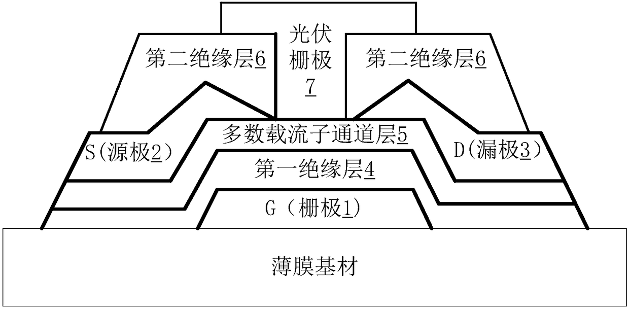
[0064] like figure 1 Shown is a cross-sectional view of an infrared light detecting film according to an embodiment of the present invention. The infrared light detection thin film includes a TFT (Thin Film Transistor) circuit area and an infrared light detection thin film transistor area, and the infrared light detection thin film transistor area is provided with an infrared photosensitive thin film transistor. The present invention mainly improves the infrared photosensitive thin film transistor to enhance the photosensitivity of the infrared photosensitive thin film transistor and improve the signal-to-noise ratio, so that the device composed of the infrared light detection thin film containing the infrared photosensitive thin film...


PUM


Abstract

The invention provides an infrared light detection thin film, device and display device and a fabrication method of the infrared light sensing thin film. Compared with a device employing a TFT leakagecurrent as an infrared photosensitive thin film transistor, a bottom gate-type field-effect transistor structure is in a way that a photovoltaic gate is arranged in a gap between a source and a drain, the photoelectron simulation is substantially improved. In each detection pixel, the source and the source are connected in parallel, the drain and the drain are also connected in parallel, adjacentsource and drain are in clearance fit, the recombination probability of electrons and holes of optical excitation is reduced, the success probability of the photoelectrons collected by an electrode under a field-effect effect is improved, and the photosensitivity of the TFT leakage current infrared light thin film transistor is improved to the maximum extent. The infrared light detection thin film can be implemented without doping boron-containing gas, the pollution to an environment during the production process of the infrared light detection thin film is effectively reduced, and the production cost is reduced.

Description

technical field [0001] The invention relates to the field of optical devices, in particular to an infrared light detection film, a device, a display device and a preparation method. Background technique [0002] A liquid crystal display (LCD) screen or an active matrix organic light emitting diode (AMOLED) display screen uses a thin film transistor (TFT) structure to scan and drive a single pixel to realize the display function of the pixel array on the screen. The main structure forming the switching function of the TFT is a semiconductor field effect transistor (FET). The main materials of the well-known semiconductor layer are amorphous silicon, polysilicon, indium gallium zinc oxide (IGZO), or organic compounds mixed with carbon nanomaterials, etc. . Since the structure of infrared photodetection diodes (Photo Diode) can also be made of such semiconductor materials, and the production equipment is also compatible with the production equipment of TFT arrays, in recent ye...

Claims


Application Information

Patent Timeline
IPC IPC(8): H01L31/0224H01L31/113H01L31/20H01L27/144
CPCH01L27/1443H01L27/1446H01L31/022408H01L31/1136H01L31/202H01L27/14669G01J5/20G02F1/13338H10K59/60H01L31/0224H01L27/144H01L31/113Y02E10/50H01L31/09H01L31/101H01L31/18H01L31/109H01L31/1129H01L31/1127
Inventor 黄建东
Owner SHANGHAI HARVEST INTELLIGENCE TECH CO LTD
Why Eureka
Try Eureka