Preparation method of selective emitter of solar cell

A solar cell and selective technology, applied in circuits, photovoltaic power generation, electrical components, etc., can solve the problems affecting the performance of solar cells and high surface concentration, and achieve the effect of low surface concentration, simple process, shallow junction and deep junction

Inactive Publication Date: 2019-03-08
北京晶澳太阳能光伏科技有限公司
View PDF8 Cites 4 Cited by
  • Summary
  • Abstract
  • Description
  • Claims
  • Application Information

AI Technical Summary

Problems solved by technology

However, the surface concentration of the lightly doped region in the selective emitter prepared by the existing one-step diffusion method is high, which affects the performance of the solar cell

Method used


Image

  • Preparation method of selective emitter of solar cell
  • Preparation method of selective emitter of solar cell
  • Preparation method of selective emitter of solar cell

Examples


Embodiment 1

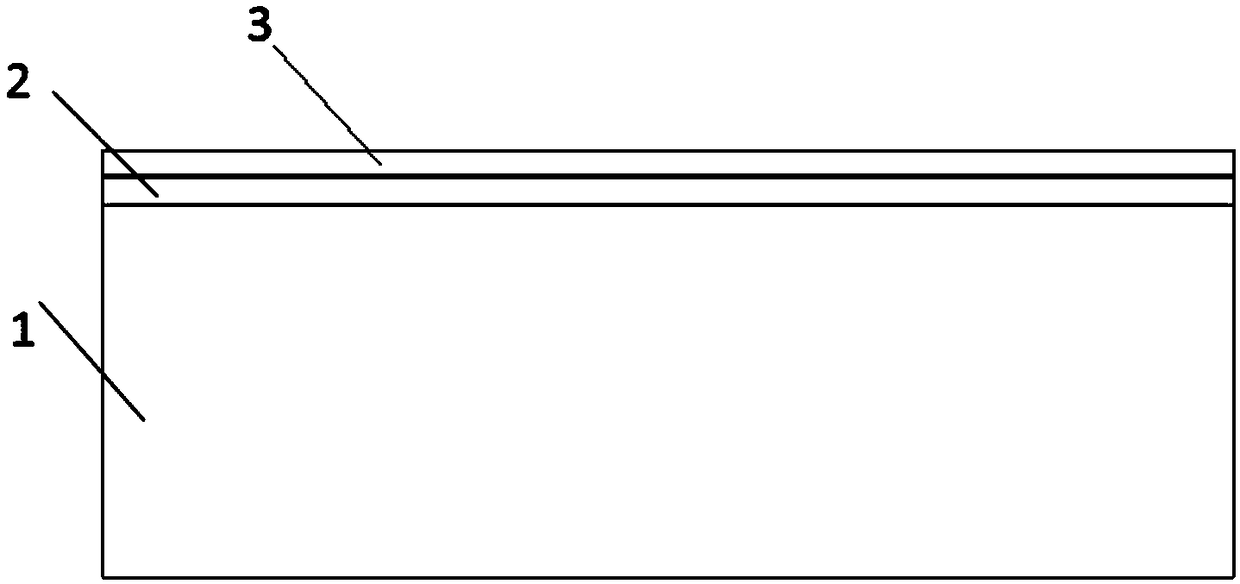
[0044] This embodiment provides a method for preparing a selective emitter of a solar cell, using a silicon oxide film with a thickness of 1.5 nm and a polysilicon film with a thickness of 200 nm as the doped filter layer, which specifically includes the following steps.

[0045] Step 101, using HCl+H 2 O 2 The solution and hydrofluoric acid clean the P-type silicon substrate 1 after texturing;

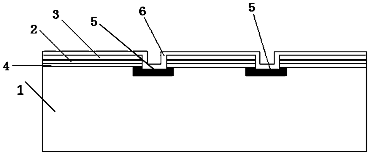
[0046] Step 102, using low pressure chemical vapor deposition (LPCVD) to sequentially grow a layer of silicon oxide film 2 with a thickness of 1.5 nm and a layer of polysilicon film 3 with a thickness of 200 nm on the entire surface of the cleaned silicon substrate 1 (the growth temperature is 610℃), that is, the silicon oxide film 2 is located between the polysilicon film 3 and the silicon substrate 1, such as figure 1 Shown

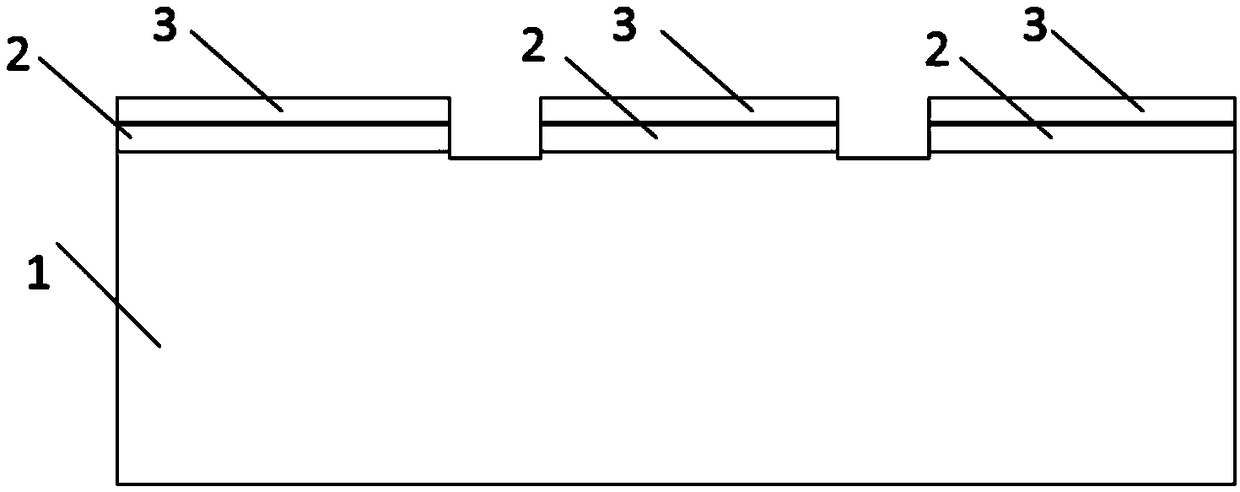
[0047] Step 103, according to the pattern design of the metal contact electrode, use a picosecond laser to remove the silicon oxide film 2 and the polysilicon film 3 ...

Embodiment 2

[0053] This embodiment provides a method for preparing a selective emitter of a solar cell, which uses a silicon oxide film with a thickness of 0.5 nm and a microcrystalline silicon film with a thickness of 300 nm as the doped filter layer, which specifically includes the following steps.

[0054] Step 201, using HCl+H 2 O 2 Solution and hydrofluoric acid clean the N-type silicon substrate after texturing;

[0055] Step 202, using plasma-enhanced chemical vapor deposition (PECVD) to sequentially grow a layer of silicon oxide film with a thickness of 0.5 nm and a layer of microcrystalline silicon film with a thickness of 300 nm on the entire surface of the cleaned silicon substrate (the growth temperature is 600℃), that is, the silicon oxide film is located between the microcrystalline silicon film and the silicon substrate;

[0056] Step 203, according to the pattern design of the metal contact electrode, use a picosecond laser to remove the silicon oxide film and the microcrystallin...

Embodiment 3

[0062] This embodiment provides a method for preparing a selective emitter of a solar cell, which uses a silicon oxide film with a thickness of 2.5 nm and an amorphous silicon film with a thickness of 500 nm as the doped filter layer, which specifically includes the following steps.

[0063] Step 301, using HCl+H 2 O 2 Solution and hydrofluoric acid clean the N-type silicon substrate after texturing;

[0064] Step 302, using low pressure chemical vapor deposition (LPCVD) to sequentially grow a silicon oxide film with a thickness of 2.5 nm and an amorphous silicon film with a thickness of 500 nm (growth temperature is 590) on the entire surface of the cleaned silicon substrate. °C), that is, the silicon oxide film is located between the amorphous silicon film and the silicon substrate;

[0065] Step 303, according to the pattern design of the metal contact electrode, use a picosecond laser to remove the silicon oxide film and the amorphous silicon film on the metal contact area on the...


PUM


Abstract

The invention discloses a preparation method of a selective emitter of a solar cell. The method can obtain a lightly-doped emitter region with lower surface concentration, shallower junction depth andhigher sheet resistance, thus an emitter with better performance can be obtained. The preparation method of the selective emitter of the solar cell comprises the following steps: (1) providing a silicon substrate, wherein the surface of the silicon substrate comprises a metal contact region used for being contacted with a metal contact electrode and a non-metal contact region located outside themetal contact region; (2) arranging a doped filter layer on the non-metal contact region of the surface of the silicon substrate, wherein the doped filter layer includes a silicon thin film; and (3) doping the silicon substrate, forming a lightly doped region of the selective emitter in the non-metal contact region, provided with the doped filter layer, on the surface of the silicon substrate, andforming a heavily doped region of the selective emitter in the metal contact region, provided with no doped filter layer, on the surface of the silicon substrate.

Description

Technical field [0001] The invention belongs to the field of solar photovoltaic components, and specifically relates to a method for preparing a selective emitter of a solar cell. Background technique [0002] Solar cells are semiconductor devices that convert light energy into electrical energy. Lower production costs and higher energy conversion efficiency have always been the goals pursued by the solar cell industry. To obtain a high-efficiency solar cell, the surface must have good passivation and a low surface recombination rate, so as to obtain a higher opening voltage, current and efficiency. In the existing ordinary crystalline silicon solar cell manufacturing technology, uniformly doped emitters are generally used. In order to reduce the surface recombination of the emitter and improve the short-wave response of the crystalline silicon solar cell, the surface doping concentration of the emitter must be reduced; however, in order to reduce the metal contact recombination...

Claims


Application Information

Patent Timeline
Patent Type & Authority Applications(China)
IPC IPC(8): H01L31/18H01L31/068
CPCH01L31/068H01L31/1804Y02E10/547Y02P70/50
Inventor 张俊兵张峰周艳方
Owner 北京晶澳太阳能光伏科技有限公司
Why Eureka
Try Eureka