A method of laser processing chip

A laser processing and chip technology, used in metal processing equipment, laser welding equipment, manufacturing tools, etc., can solve the problems of easy damage to the bottom readout circuit, damage to the bottom readout circuit, complicated corrosion process, etc., to eliminate position offset. Influence, high processing speed, small heat-affected zone effect

Active Publication Date: 2021-09-03
北京中科镭特电子有限公司
View PDF8 Cites 0 Cited by
  • Summary
  • Abstract
  • Description
  • Claims
  • Application Information

AI Technical Summary

Problems solved by technology

The advantages of this method: simple operation, low equipment requirements, and good etching selectivity; disadvantages: first, a photolithography process is required for each chip, which is time-consuming and laborious; Liquid, complex corrosion process, low precision, easy to damage the bottom readout circuit
The advantages of dry etching: the first etching selectivity and anisotropy are good, the second etching pattern can be precisely controlled and the resolution is high; the disadvantages: first, a single chip needs to be photolithography, which is time-consuming and laborious, and the second is damage Bottom readout circuit

Method used


Image

  • A method of laser processing chip
  • A method of laser processing chip
  • A method of laser processing chip

Examples


Embodiment 1

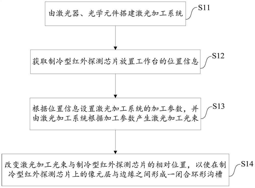
[0048] Embodiments of the present invention provide a method for laser processing chips, such as figure 1 As shown, the method includes:

[0049] S11. Build a laser processing system with lasers and optical components;

[0050] S12. Acquiring the position information of the workbench where the cooled infrared detection chip is placed;

[0051] S13. Set the processing parameters of the laser processing system according to the position information, and generate the laser processing beam according to the processing parameters by the laser processing system;

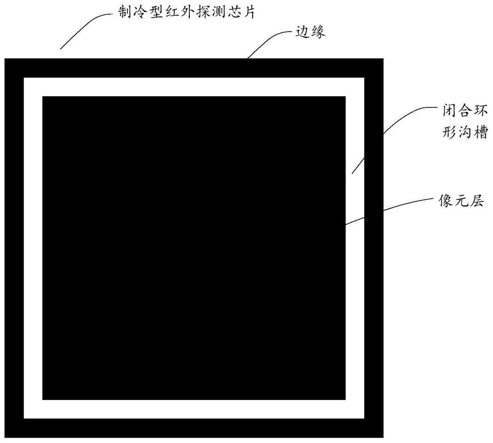
[0052] S14. Changing the relative position of the laser processing beam and the cooled infrared detection chip, so that a closed annular groove is formed between the pixel layer and the edge on the cooled infrared detection chip.

[0053] The laser processing chip method provided by the embodiment of the present invention mainly uses the laser processing system to generate a laser beam to prepare a closed annular groove on...

Embodiment 2

[0079] An embodiment of the present invention provides a device for laser processing chips, such as Figure 2 to Figure 4 As shown, the device includes:

[0080] Workbench, used to place the refrigerated infrared detection chip to be processed;

[0081] The control system is used to obtain the position information of the cooling type infrared detection chip placed on the workbench, and then set the processing parameters of the laser processing system according to the position information, and control the laser processing system to generate the laser processing beam according to the processing parameters;

[0082] The laser processing system is formed by a laser, a beam expander and collimator, and a galvanometer. It is used to expand and collimate the laser processing beam emitted by the laser through the beam expander and collimator, and then change the laser processing beam through the galvanometer. The relative position of the cooling type infrared detection chip is such t...

Embodiment 3

[0118] Since the cutting of infrared semiconductor materials by ultrashort pulse laser is mainly realized through the multiphoton absorption mechanism, the process of plasma recombination is often accompanied by the generation of dust and smoke. Inhaling a large amount of dust and the generated gas is not only harmful to the human body, but also has a bad impact on the mechanical and optical transmission, laser performance, etc. Therefore, these additional harmful substances are efficiently removed.

[0119] An embodiment of the present invention provides a device for laser processing chips, such as Image 6 As shown, the device includes:

[0120] Workbench, used to place the refrigerated infrared detection chip to be processed;

[0121] The dust removal device is arranged between the laser processing system and the workbench and establishes a processing chamber on the workbench, which is used to feed auxiliary gas into the processing chamber so that the processing chamber is...


PUM

PropertyMeasurementUnit
wavelengthaaaaaaaaaa

Abstract

The invention provides a method for laser processing chips, comprising: building a laser processing system with lasers and optical elements; obtaining the position information of the cooling type infrared detection chip placed on the workbench; setting the processing parameters of the laser processing system according to the position information, and using the laser The processing system generates a laser processing beam according to the processing parameters; changing the relative position of the laser processing beam and the cooled infrared detection chip, so that a closed annular groove is formed between the pixel layer and the edge on the cooled infrared detection chip. The invention can evenly reduce the pulling of the overflowing filling glue around the pixel layer on the cooling type infrared detection chip when the temperature cycle passes, and then can efficiently and uniformly eliminate the thermal stress on the photosensitive layer and epoxy resin of the cooling type infrared detection chip Position offset effects between layers.

Description

technical field [0001] The invention relates to the technical field of laser micromachining, in particular to a method for laser machining chips. Background technique [0002] Infrared detectors have been well used in both civil and military applications, and the performance of cooled infrared detectors is particularly excellent. The infrared detection chip in the cooling type infrared detector is often in an environment with drastic temperature changes. In order to ensure its normal working performance, the infrared detection chip in the detector needs to be cooled with liquid nitrogen during the working state. The temperature at this time is about It is -200°C, but during non-working hours, the infrared detection chip is exposed to the atmospheric temperature. For example, the highest temperature in the desert can sometimes reach about 70°C, so the ambient temperature of the infrared detection chip is between -200°C and Constantly changing between 70°C. [0003] The stru...

Claims


Application Information

Patent Timeline
Patent Type & Authority Patents(China)
IPC IPC(8): B23K26/364B23K26/064B23K26/70B23K26/16
CPCB23K26/0643B23K26/0648B23K26/16B23K26/064B23K26/364B23K26/702
Inventor 李纪东侯煜张紫辰
Owner 北京中科镭特电子有限公司
Why Eureka
Try Eureka