Preparation method of thin film transistor, array substrate and liquid crystal display panel
A technology of thin film transistors and array substrates, which is applied in the field of microelectronics, can solve the problems of insufficient voltage resistance of thin film transistor devices, electrostatic breakdown, and low reliability of thin film transistors, and achieve strong breakdown resistance, improve voltage resistance, and not easily The effect of electrostatic breakdown
- Summary
- Abstract
- Description
- Claims
- Application Information
AI Technical Summary
Problems solved by technology
Method used
Image
Examples
Embodiment 1
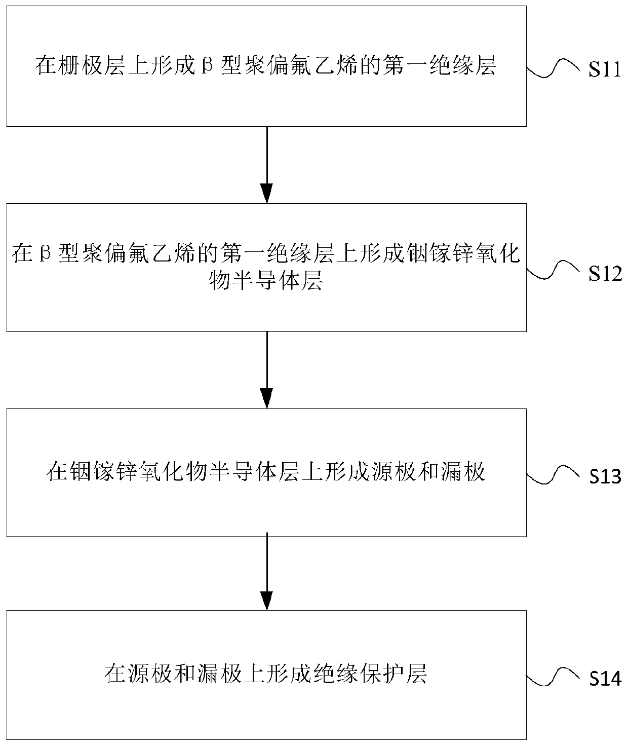
[0036] figure 1 It is a schematic flow chart of the manufacturing method of the thin film transistor provided in Embodiment 1 of the present invention. Such as figure 1 As shown, the preparation method of the thin film transistor provided in this embodiment may specifically include the following steps:
[0037] S11, forming a first insulating layer of β-type polyvinylidene fluoride on the gate layer.
[0038] S12, forming an indium gallium zinc oxide semiconductor layer on the first insulating layer of β-type polyvinylidene fluoride;
[0039] S13, forming a source electrode and a drain electrode on the indium gallium zinc oxide semiconductor layer;
[0040] S14, forming an insulating protection layer on the source and the drain.
[0041] Specifically, the characteristics of the indium gallium zinc oxide semiconductor layer in the thin film transistor are easily affected by ultraviolet light, water vapor and impurity ions, and the characteristics such as threshold voltage d...
Embodiment 2
[0054] Figure 2a ~ Figure 2e It is a schematic diagram showing the detailed process of the thin film transistor manufacturing method of the present invention. On the basis of Embodiment 1, this embodiment cites specific examples, and further explains the process conditions and process parameters of each step in the foregoing Embodiment 1. For the same part as Embodiment 1, here No longer.
[0055] The preparation method of the thin film transistor of this embodiment comprises the following steps:
[0056] 1) Using an ultrasonic cleaner, first clean the 10cm×10cm×0.5mm glass substrate 1 ultrasonically with acetone or alcohol for 30 minutes to remove surface organic matter and large particles, then take it out and wipe it with a clean cloth with alcohol, and then clean it with pure Rinse with water for 5 minutes, and blow with nitrogen gas until it is dried for use.
[0057] 2) if Figure 2a As shown, on the glass substrate 1 after step 1) cleaning, the gate layer 2 is prep...
Embodiment 3
[0065] On the basis of Embodiment 1, this embodiment cites specific examples, and further explains the process conditions and process parameters of each step in the foregoing Embodiment 1. For the same part as Embodiment 1, here No longer.
[0066] The preparation method of the thin film transistor of this embodiment comprises the following steps:
[0067] 1) Using an ultrasonic cleaner, first clean the 10cm×10cm×0.5mm glass substrate 1 ultrasonically with acetone or alcohol for 30 minutes to remove surface organic matter and large particles, then take it out and wipe it with a clean cloth with alcohol, and then clean it with pure Rinse with water for 5 minutes, and blow with nitrogen gas until it is dried for use.
[0068] 2) if Figure 2a As shown, on the cleaned glass substrate 1 in step 1), the gate layer 2 is prepared by using the magnetron sputtering coating process. Specifically, a 30nm metal Ti layer is first formed, and a 170nm metal Cu layer is formed on the Ti lay...
PUM
| Property | Measurement | Unit |
|---|---|---|
| thickness | aaaaa | aaaaa |
| thickness | aaaaa | aaaaa |
| thickness | aaaaa | aaaaa |
Abstract
Description
Claims
Application Information


