SPAD with high detection efficiency and low dark count based on standard CMOS process

A detection efficiency and process technology, applied in the direction of electrical components, circuits, semiconductor devices, etc., can solve the problem that the detection efficiency is only 15%, achieve the effects of reducing tunneling dark counts, facilitating light absorption, and reducing electrical crosstalk

Inactive Publication Date: 2019-04-16
TIANJIN UNIV
View PDF4 Cites 18 Cited by
  • Summary
  • Abstract
  • Description
  • Claims
  • Application Information

AI Technical Summary

Problems solved by technology

E. Kamrani and others designed a high-gain SPAD structure, although the

Method used


Image

  • SPAD with high detection efficiency and low dark count based on standard CMOS process
  • SPAD with high detection efficiency and low dark count based on standard CMOS process
  • SPAD with high detection efficiency and low dark count based on standard CMOS process

Examples


Embodiment 1

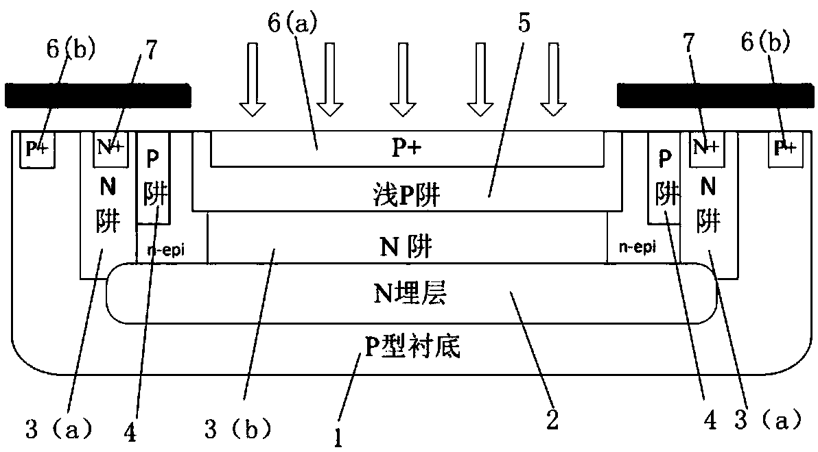
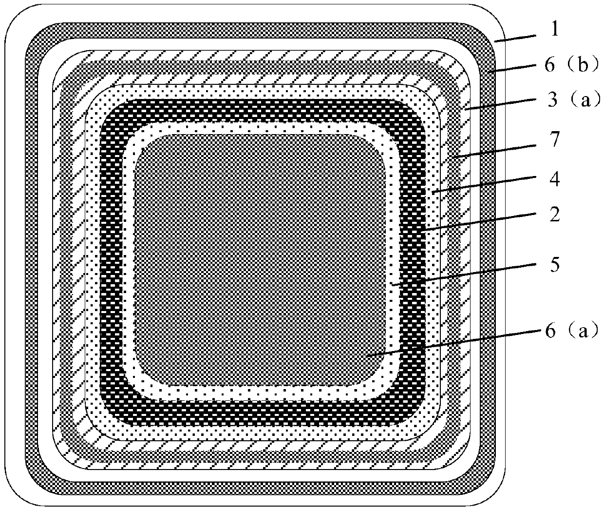
[0029] The embodiment of the present invention proposes a single photon avalanche diode detector structure with high detection efficiency, low dark count and compatible with standard CMOS technology, see figure 1 And figure 2 The floor plan, see the description below for details:

[0030] The detector is mainly composed of heavily doped P + Region, shallow P well region and N-type diffusion region together constitute P + The photosensitive PN junction formed by the P / N well, two P-type injections of different concentrations form a gradual junction, which greatly reduces the dark count of tunneling. The N buried layer 2 has the characteristics of an inverted doping distribution, and the surface doping increases with the increase in depth to form a virtual guard ring, which forms a double guard ring structure with the P well guard ring to improve the reliability and detection performance of the device.

[0031] When the device is working, due to the low doping concentration of the N-...

Embodiment 2

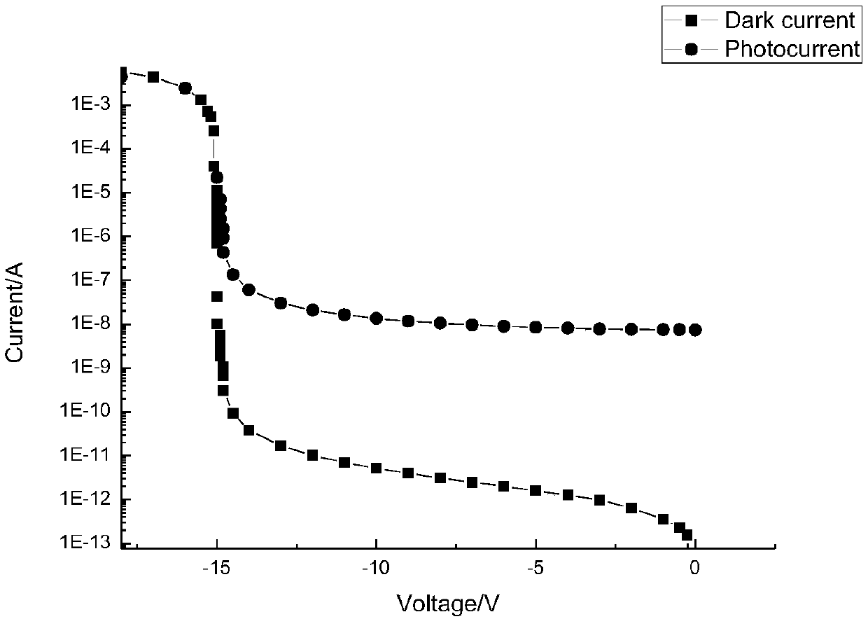
[0033] The following combines specific experimental data (attached Figure 1-5 ), the solution in embodiment 1 is further explained, see the following description for details:

[0034] figure 1 It is the structure diagram of the low dark count SPAD photodetector based on standard CMOS process according to the embodiment of the present invention, with an area of ​​13×13μm 2 As an example, the specific structure of the photodetector in the embodiment of the present invention is as follows:

[0035] 1) Part 1 in the figure is the P-type substrate of the detector. The material of the P-type substrate 1 is a lightly doped P-type silicon wafer. The P-type substrate 1 serves as a supporting base of the detector according to the embodiment of the present invention;

[0036] 2) Part 2 in the figure is the N buried region. Due to the unique doping characteristics of the N buried layer 2, two doping concentrations under different junction depths are used for calculation, and the concentration...


PUM


Abstract

The invention discloses an SPAD with high detection efficiency and low dark count based on a standard CMOS process. The SPAD is prepared on a P substrate that is provided based on the CMOS process; anN-buried layer is arranged on the P substrate to play an isolation role, the buried N-type injection has the characteristic of inverted doping distribution, the doping concentration increases with the increase of depth, and a virtual protection ring is formed; an N-well region, a P-well region and a heavily doped P+ region are respectively arranged in a diffusion doping region of the N-buried layer, and the N-well region is taken as a component part of a photosensitive PN junction; the P-well region serves as a protection ring; the heavily doped P+ region, a shallow P-well region and the N-type region jointly form a P+P-/N-well photosensitive PN junction, and the combination of two P-type injections with different concentrations form a gradient junction to reduce the dark count of devices; the depletion region of the PN junction is the main occurrence region of avalanche multiplication, and meanwhile, the heavily doped P+ region is also taken as an anode contact region of a photodetector; an N-well contact region is arranged in the N-well region at the edge, and the N-well contact region is a heavily doped N+ region and serves as a cathode contact region of the photodetector.

Description

Technical field [0001] The invention relates to the field of photoelectric detection and photoelectric sensors, in particular to a SPAD with high detection efficiency and low dark count based on a standard CMOS process. Background technique [0002] As a detection technology for extremely weak light signals, single-photon detection has broad application prospects in the fields of quantum communication, astronomical photometry, medical imaging and radar detection. In view of its huge scientific research value and strategic position, single-photon detection has become the current One of the hot spots in the field of photoelectric detection. As the core component of the detection system, the single-photon detector determines the performance parameters of the entire single-photon detection system. Therefore, designing a miniature single-photon detector with high detection efficiency and low dark count is one of the key issues that need to be solved urgently. [0003] The traditional s...

Claims


Application Information

Patent Timeline
IPC IPC(8): H01L31/0352H01L31/107
CPCH01L31/035272H01L31/107
Inventor 谢生王雪飞毛陆虹
Owner TIANJIN UNIV
Why Eureka
Try Eureka