Laminated solar cell top cell and preparation method thereof

A stacked solar and top cell technology, applied in the field of solar cells, can solve the problems of low photoelectric conversion efficiency, low band gap, lead-containing perovskite, etc., and achieve rich crust content, high band gap, Effect of low antisite defect density

Inactive Publication Date: 2019-04-23
CENT SOUTH UNIV
View PDF5 Cites 3 Cited by
  • Summary
  • Abstract
  • Description
  • Claims
  • Application Information

AI Technical Summary

Problems solved by technology

However, CIGS and CdTe have low bandgap widths, are not suitable as top cells, and contain elements that are not rich and toxic; while CZTS, a non-toxic and harmless thin-film solar cell with a high bandgap width (1.5eV), is subject to Influenced by anti-site defects, the photoelectric conversion efficiency has not been improved
At present, the stacked cells of perovskite solar cells and silicon solar cells have attracted much attention, but the disadvantages of lead, a toxic element, and poor stability in perovskite limit its development.

Method used


Image

  • Laminated solar cell top cell and preparation method thereof
  • Laminated solar cell top cell and preparation method thereof
  • Laminated solar cell top cell and preparation method thereof

Examples


Embodiment 1

[0033] Cut FTO glass (light transmittance ≥ 90%) into 1.5cm×2.0cm, then use glass cleaning agent to clean FTO glass, soak it in deionized water containing glass cleaning agent, acetone, alcohol, deionized Sonicate in water for 15 minutes, and blow dry with high-purity nitrogen to obtain a clean FTO conductive glass substrate.

[0034] Use ZnSO 4 , ammonia water and thiourea were used to prepare a layer of ZnS electron transport layer on the FTO conductive glass substrate by chemical water bath method at 80°C. The film had a bandgap width of 3.4eV and a thickness of about 60nm.

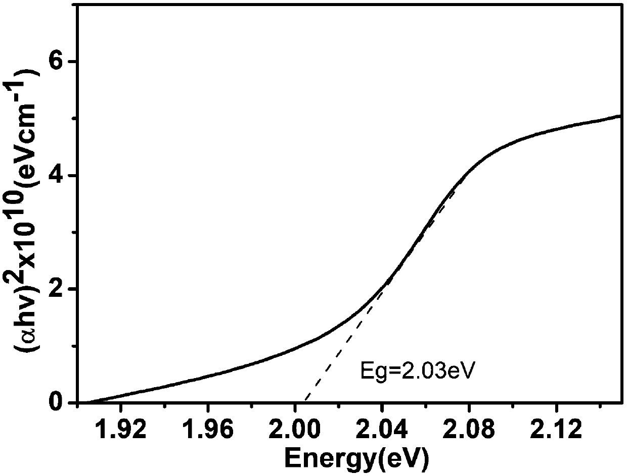
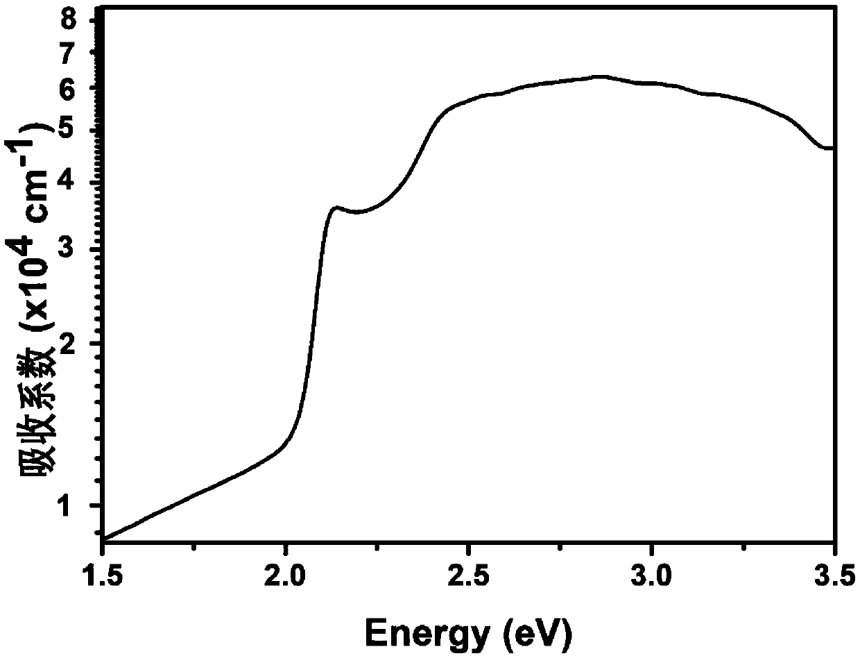
[0035] Prepare a layer of CBTS light absorption layer on the above-mentioned ZnS electron transport layer by sol-gel method; at the same time, in order to measure the forbidden band width and light absorption coefficient of the CBTS, prepare a CBTS film on a piece of white glass with the same size and cleaned according to the above method . The above two pieces of glass were annealed at 500°C for 60 ...

Embodiment 2

[0039] On the cleaned ITO transparent conductive glass substrate (light transmittance ≥ 90%), a layer of Zn(O, S) electron transport layer was prepared by ZnO and ZnS double target co-sputtering method, which can be adjusted by adjusting ZnO and ZnS The sputtering power of the target changes the ratio of O and S in the material to achieve the purpose of controlling the band gap. The final Zn(O, S) band gap is 3.05eV and the thickness is 30nm.

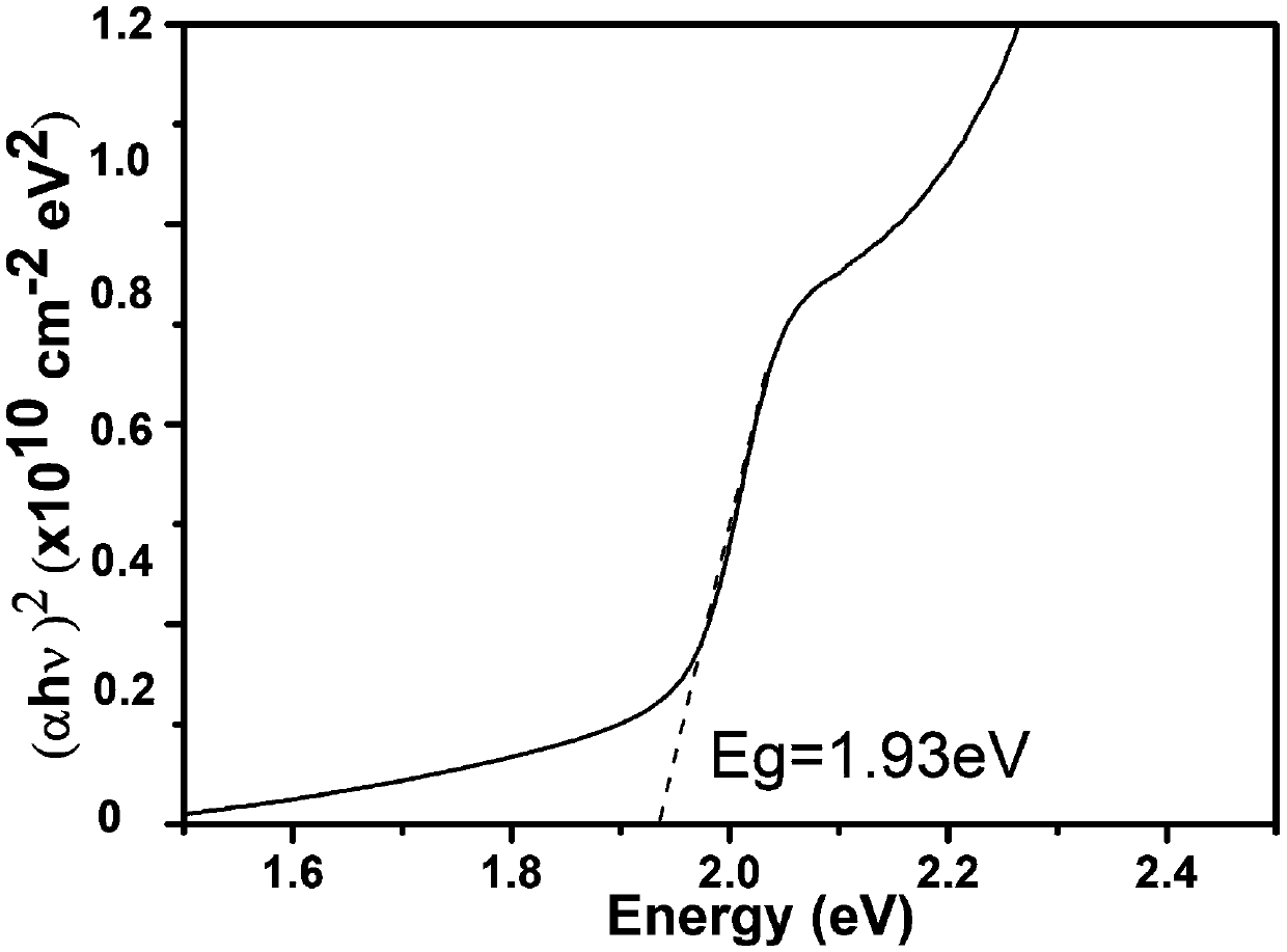
[0040]Then use the sol-gel method to prepare one deck of CSTS light-absorbing layer on the above-mentioned Zn (O, S) electron transport layer; simultaneously in order to measure the forbidden band width and light absorption coefficient of this CBTS thin film, in a piece of the same size, according to embodiment 1 CSTS thin films were prepared on cleaned white glass as in the method. The above two pieces of glass were annealed at 400°C for 40 minutes in a sulfide atmosphere.

[0041] Then a layer of FTO transparent top electrode was fab...

Embodiment 3

[0044] On the cleaned ATO transparent conductive glass substrate, a layer of ZnS electron transport layer was prepared by sputtering method, and then a layer of CBTS light absorption layer was prepared by sputtering method. A layer of ITO transparent top electrode was prepared by magnetron sputtering. The thicknesses of the ZnS electron transport layer, the CBTS light absorption layer, and the ITO transparent top electrode are measured to be about 80nm, 700nm, and 150nm, respectively.

[0045] Such as Figure 5 As shown, the photoelectric conversion performance of the above device was measured, and the open circuit voltage was 0.7V, and the short circuit current density was 5.25mA / cm 2 , The photoelectric conversion efficiency is 1.72%. It can be seen that the open circuit voltage of 0.7V is significantly higher than the open circuit voltage of the current 12.6% world record CZTSSe device (less than 0.6V), indicating that CBTS is a very suitable light absorbing layer materia...


PUM


Abstract

The invention discloses a laminated solar cell top cell and a preparation method thereof. The laminated solar cell top cell comprises a transparent conductive glass substrate, an electron transmissionlayer, a Cu2BaSnS4 or Cu2SrSnS4 light absorption layer and a transparent top electrode in sequential laminated arrangement. The forbidden bandwidth of the Cu2BaSnS4 or Cu2SrSnS4 material is high; thelight absorption coefficient is high. Compared with conventional CZTS, lower inverse defect density is realized; higher open circuit voltage can be obtained; the material is very suitable to be usedas light absorption layer materials of the laminated solar cell top cell. The laminated solar cell top cell has the advantages that the structure is simple; the composition elements are nontoxic and harmless; the stability is high, and the preparation method is simple and easy.

Description

technical field [0001] The invention relates to the technical field of solar cells, in particular to a stacked solar cell top cell and a preparation method thereof. Background technique [0002] Solar energy is an inexhaustible clean energy, which is of great significance to human beings to solve global important problems such as resource crisis and environmental degradation. Solar cells can convert solar energy into electrical energy and realize efficient utilization of solar energy. At present, silicon solar cells are the mainstream of solar cells, occupying 90% of the market, and their highest efficiency reaches more than 25%. New solar cells such as thin-film solar cells and perovskite solar cells have also achieved good development. For example, Both CIGS and CdTe thin-film solar cells have achieved a photoelectric conversion efficiency of more than 20%, and perovskite solar cells have also increased their photoelectric conversion efficiency to more than 20% in a very ...

Claims


Application Information

Patent Timeline
Patent Type & Authority Applications(China)
IPC IPC(8): H01L31/032H01L31/0336H01L31/0445H01L31/0725H01L31/18
CPCH01L31/0327H01L31/0336H01L31/0445H01L31/0725H01L31/18Y02E10/50Y02P70/50
Inventor 肖涵睿肖劲刘芳洋蒋良兴贾明
Owner CENT SOUTH UNIV
Why Eureka
Try Eureka