
Processing method for surface modification and metallization of hole walls of ceramic circuit board

A technology for ceramic circuit boards and surface modification, which is applied in circuit substrate materials, printed circuits, and printed circuit manufacturing. problems, to achieve the effect of reducing the subsequent plating time, improving the plating efficiency, and meeting the requirements of mass production

Inactive Publication Date: 2019-04-26
HUIZHOU KING BROTHER CIRCUIT TECH
View PDF5 Cites 1 Cited by
  • Summary
  • Abstract
  • Description
  • Claims
  • Application Information

AI Technical Summary

Problems solved by technology

[0007] A. It needs to use expensive vacuum plating equipment, which is not available in general PCB factories; at the same time, the processing cost is high and it does not have a competitive advantage;
[0008] B. The adhesion of vacuum electroplated copper on the ceramic surface is not good, and it is not as good as the adhesion of high-temperature sintered copper foil;
[0009] C. The thickness of vacuum electroplating copper is very thin, and it takes a long time to electroplate to thicken afterwards. When the customer needs 100-200um thick copper, the electroplating time is as long as more than 5H, which is inefficient and cannot meet the requirements of batch processing.

Method used


Image

  • Processing method for surface modification and metallization of hole walls of ceramic circuit board

Examples


Embodiment 1

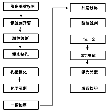
[0058] A processing method for surface modification and metallization of a hole wall of a ceramic circuit board, characterized in that the double-sided ceramic board includes an intermediate ceramic layer and copper clad layers arranged on both sides of the ceramic layer; comprising the following steps:

[0059] S1. Ceramic substrate preparation;

[0060] S2. Pre-etched windows before laser drilling;

[0061] S3. Hole metallization, electroless copper deposition after laser drilling;

[0062] The step S2 includes the following specific steps:

[0063] S21. File design, design the window file at the metallized hole;

[0064] S22. Partially open the window, first paste the dry film on the whole board, then expose it with the window file, and expose the copper surface after development;

[0065] S23. Partial etching, etching away the copper surface of the window to expose the ceramic substrate;

[0066] S24. Electroplating is thickened, the whole board is electroplated, and the...

Embodiment 2

[0075] A processing method for surface modification and metallization of a hole wall of a ceramic circuit board, characterized in that it comprises the following steps:

[0076] A. Ceramic substrate preparation;

[0077] B. Production of engineering documents, in addition to designing conventional drilling, circuit, test and shape documents, add pre-etching window opening documents, the pre-etching window opening documents are pre-etched on the metallized hole parts of the ceramic plate before laser drilling The copper surface is designed with a window as large as the hole;

[0078] C. Pre-etched windows;

[0079] D. Laser drilling, according to the MI drilling file, using laser processing to drill through holes;

[0080] E. Coarsening of the hole wall;

[0081] F. Hole metallization: metallize the hole wall according to the traditional electroless copper deposition method;

[0082] G. Copper electroplating: Electroplate the thickness of hole copper and surface copper to ...

Embodiment 3

[0095] A processing method for surface modification and metallization of a hole wall of a ceramic circuit board, characterized in that it comprises the following steps:

[0096] A. Ceramic substrate preparation;

[0097] B. Production of engineering documents, in addition to designing conventional drilling, circuit, test and shape documents, add pre-etching window opening documents, the pre-etching window opening documents are pre-etched on the metallized hole parts of the ceramic plate before laser drilling The copper surface is designed with a window as large as the hole;

[0098] C. Pre-etched windows;

[0099] D. Laser drilling, according to the MI drilling file, using laser processing to drill through holes;

[0100] E. Coarsening of the hole wall;

[0101] F. Hole metallization: metallize the hole wall according to the traditional electroless copper deposition method;

[0102] G. Copper electroplating: Electroplate the thickness of hole copper and surface copper to ...


PUM

PropertyMeasurementUnit
hardnessaaaaaaaaaa

Abstract

The invention provides a processing method for surface modification and metallization of hole walls of a ceramic circuit board. The processing method is characterized in that the double-sided ceramicboard comprises a middle ceramic layer and copper-clad layers arranged on two sides of the ceramic layer. The method comprises the following steps: S1, preparing a ceramic substrate; S2, pre-etching and windowing before laser drilling; S3, metallizing holes and conducting chemical copper deposition after laser drilling. According to the processing method, copper-clad high-temperature sintered ceramic is used as a base material for processing, so that good attachment of the original base copper is ensured; meanwhile, an appropriate copper foil thickness can be selected according to customers' requirements, subsequent electroplating time is shortened, and electroplating efficiency is maximumly improved.

Description

technical field [0001] The invention belongs to the technical field of circuit board processing, and in particular relates to a processing method for surface modification and metallization of hole walls of ceramic circuit boards. Background technique [0002] Ceramic substrates have excellent temperature resistance, chemical resistance, dimensional stability and high thermal conductivity, so they have irreplaceable technical status in some special fields; ceramic substrates commonly used in the industry are made of aluminum oxide or nitride Aluminum is the main material, and the surface of the substrate can be sintered copper foil at high temperature or vacuum electroplated copper after special treatment; the hardness of the ceramic substrate is very high, reaching more than 1500HV, which exceeds the hardness of many alloy drills, so it is difficult to use conventional mechanical drilling methods To achieve hole processing, the current common practice in the industry is to...

Claims


Application Information

Patent Timeline
Patent Type & Authority Applications(China)
IPC IPC(8): H05K3/42H05K1/03
CPCH05K1/0306H05K3/423
Inventor 唐宏华林映生陈春胡光辉卫雄李光平吴军权
Owner HUIZHOU KING BROTHER CIRCUIT TECH
Learn More