Flexible temperature-sensitive pressure sensor based on nanoparticl lattice quantum conductance and assembly method and application thereof
A pressure sensor and nanoparticle technology, applied in the direction of nanotechnology thermometers, applications of thermometers, nanotechnology for sensing, etc., can solve the problems of insufficient sensitivity and limited resolution, and achieve simplified sensing structure and functional The effect of low consumption
- Summary
- Abstract
- Description
- Claims
- Application Information
AI Technical Summary
Problems solved by technology
Method used
Image
Examples
Embodiment 1
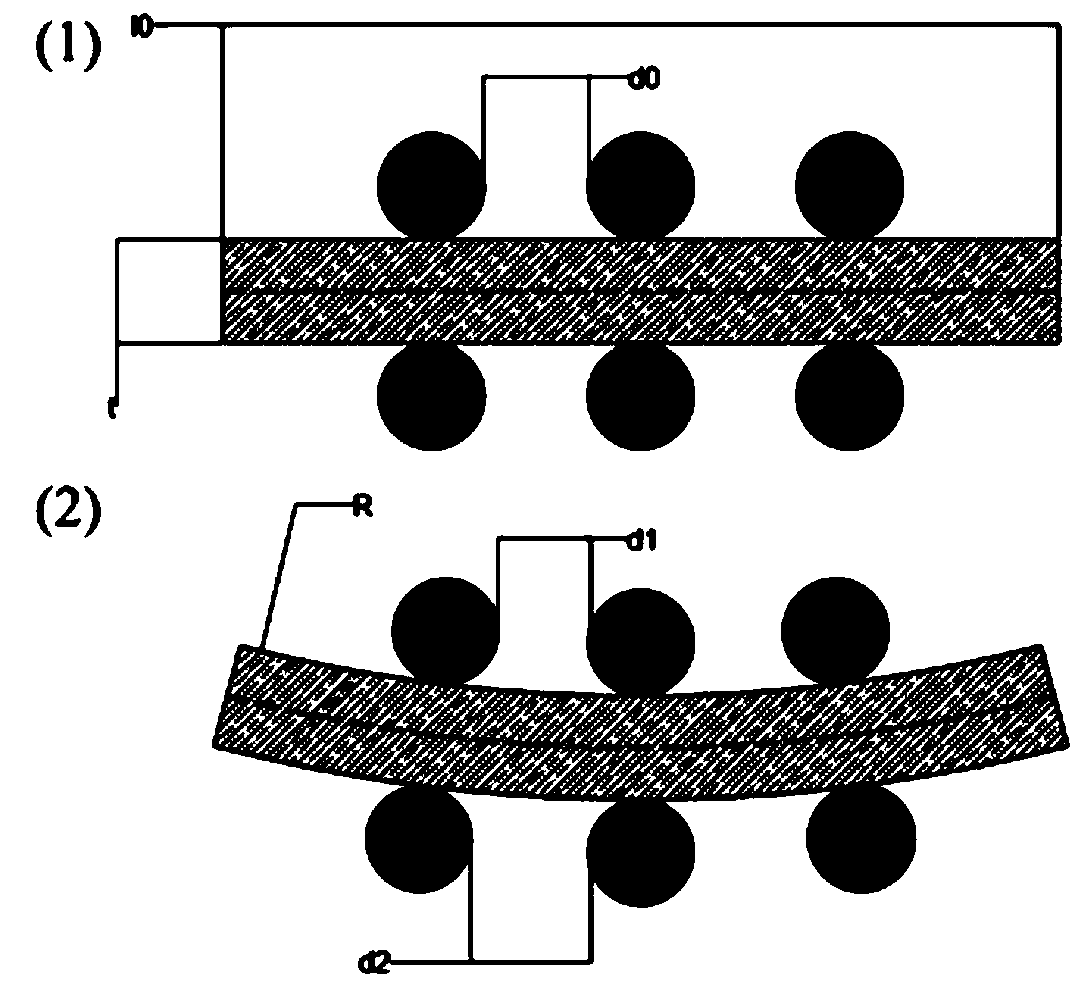
[0031] The different effects of pressure on the conductance change trend of each group of sensor lattices are deduced from the following physical principles.
[0032] Suppose the flexible film has a thickness t and a length l 0 The initial average gap of the nanoparticles in the lattice corresponding to the upper and lower surfaces of the film is d 0 , as attached figure 2 As shown in (1), when a pressure acts on the upper surface of the membrane, the flexible membrane undergoes a deformation of curvature R, from the attached figure 2 The state in (1) changes to the state in (2). At this time, the average gap between the nanoparticles on the upper surface is d 1 , the average gap between the nanoparticles on the lower surface is d 2 . In general, during the straining process, the median line of the film does not change, so the length l of the upper and lower surfaces 1 and l 2 becomes:
[0033]
[0034]
[0035] Therefore, the strains on the upper and lower sur...
Embodiment 2
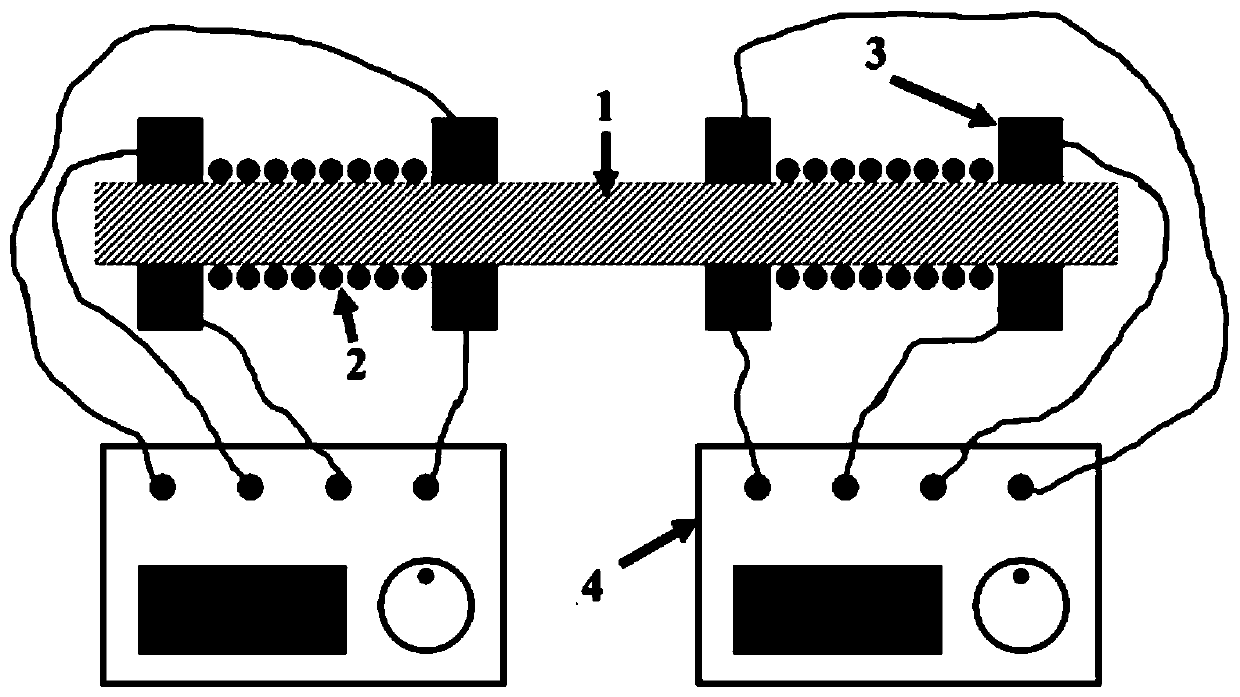
[0045] The preparation of the flexible temperature-sensitive pressure sensor based on nanoparticle lattice quantum conductance according to the present invention comprises the following steps:
[0046] Step 1. Choose a clean, smooth and scratch-free polymer insulating film. The film used is polyethylene terephthalate, and the thickness of the selected film is 0.1mm;
[0047] Step 2, printing pattern-overlapping metal conductive microelectrodes on the corresponding positions on the upper and lower surfaces of the polymer film. The microelectrode here is an interdigitated silver electrode deposited by mask evaporation in vacuum, the thickness of the metal layer is 100nm, and the gap width between the positive and negative electrodes of the electrode is 100μm;
[0048] Step 3, depositing a metal nanoparticle lattice with the same coverage between each interdigitated electrode. The metal nanoparticles are prepared by the magnetron plasma gas aggregation method, and the nanoparti...
PUM
| Property | Measurement | Unit |
|---|---|---|
| electrical resistivity | aaaaa | aaaaa |
| elastic modulus | aaaaa | aaaaa |
| size | aaaaa | aaaaa |
Abstract
Description
Claims
Application Information


