A multi-cavity coupling-enhanced nanoplasmonic laser array and its preparation method

A laser array and plasma technology, applied in the optical field, can solve the problems of high loss, low output optical power, limiting the quality factor of lasers, etc., and achieve the effect of achieving high density, increasing the output optical power, and reducing the threshold value

Active Publication Date: 2021-02-26
BEIJING UNIV OF TECH
View PDF6 Cites 0 Cited by
  • Summary
  • Abstract
  • Description
  • Claims
  • Application Information

AI Technical Summary

Problems solved by technology

However, the structure of nanoplasmonic lasers has the problem of high loss caused by metals, which limits the quality factor of the laser, resulting in a high threshold of the laser, and the output optical power of a single nanolaser is low, only at the nanowatt level

Method used


Image

  • A multi-cavity coupling-enhanced nanoplasmonic laser array and its preparation method
  • A multi-cavity coupling-enhanced nanoplasmonic laser array and its preparation method
  • A multi-cavity coupling-enhanced nanoplasmonic laser array and its preparation method

Examples


Embodiment 1

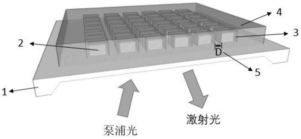
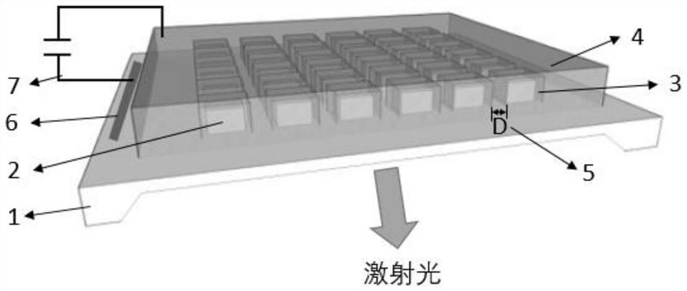
[0044] This embodiment provides a multi-cavity coupling enhanced nanoplasmonic laser array with a lasing wavelength of 1500nm, its structure is as follows figure 1 As shown, the specific materials, parameters and dimensions are as follows:

[0045] The semiconductor substrate (1) is an indium phosphide (InP) substrate;

[0046] The structure of the semiconductor gain cavity (2) is a quantum well composed of indium gallium arsenide phosphide (InGaAsP) in different proportions, the surface shape is a square, and its side length W is 320nm;

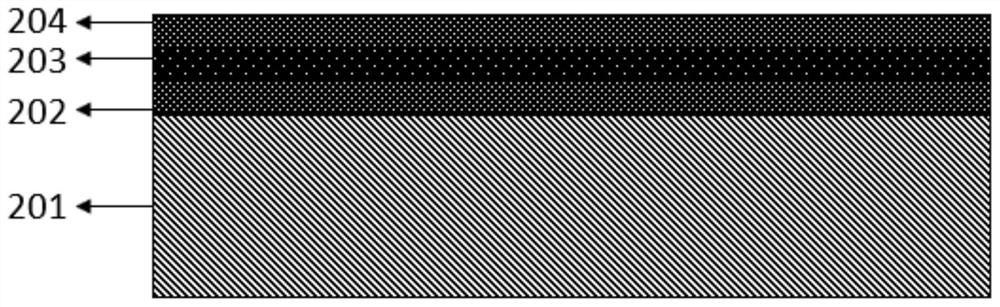
[0047] The insulating dielectric layer (3) is silicon dioxide (SiO 2 ) film 206, the thickness of which is 20nm;

[0048] The metal (4) wrapping the resonant cavity is Ti(5nm) / Ag(200nm);

[0049] The distance D(5) between the adjacent resonant cavities is 50nm.

[0050] In this embodiment, Lumerical FDTD Solutions is used to establish a corresponding model to simulate the coupling enhancement effect between the two resonators. The simulati...


PUM

PropertyMeasurementUnit
thicknessaaaaaaaaaa
thicknessaaaaaaaaaa

Abstract

A multi-cavity coupling enhanced nano-plasma laser array and a preparation method thereof belong to the field of optical technology. Comprising a semiconductor substrate, a semiconductor gain resonator, an insulating dielectric layer (3), and a metal cladding layer, there is a semiconductor gain resonator array on the semiconductor substrate, that is, an insulating medium is arranged on the surface of the semiconductor substrate and the semiconductor gain resonator array layer, the insulating dielectric layer wraps each semiconductor gain resonant cavity, and the insulating dielectric layer also maintains the pattern of the semiconductor gain resonant cavity array, that is, forms the semiconductor gain resonant cavity-insulating dielectric layer array, and is provided with a metal wrapping layer on the insulating dielectric layer , and the metal cladding layer also fills the array pattern on the insulating dielectric layer. The surface plasmon modes (evanescent waves) between adjacent resonant cavities of the present invention can be coupled with each other, thereby improving the performance of the nanometer laser and realizing the output of the ultra-high density plasma laser surface array.

Description

technical field [0001] The invention relates to a nano-laser array and its preparation, in particular to a multi-cavity coupling-enhanced nano-plasma laser array and a preparation method thereof, belonging to the field of optical technology. Mainly used in optoelectronic integration, optical communication, optical information storage, optical microscopy, super-resolution and other fields. Background technique [0002] Surface plasmons provide a way to process light at the nanoscale, that is, light waves are resonantly coupled with free electrons on the metal surface to generate near-field electromagnetic waves propagating along the metal surface, which has a strong light field confinement ability, It is one of the most effective ways to overcome the optical diffraction limit and realize local electromagnetic field enhancement. The surface plasmon-based nanolaser amplifies the surface plasmons through the gain material around the medium, and resonates in the nanoscale resona...

Claims


Application Information

Patent Timeline
Patent Type & Authority Patents(China)
IPC IPC(8): H01S5/022H01S5/40H01S5/30H01S5/10H01S5/04H01S5/042
Inventor 关宝璐张成龙杨悦吴宇辰
Owner BEIJING UNIV OF TECH
Why Eureka
Try Eureka