High-stability, low-dark-current fully inorganic perovskite photoelectric detector and preparation method thereof
A technology of photodetectors and inorganic calcium, applied in circuits, electrical components, semiconductor devices, etc., can solve the problems of inability to obtain high-quality crystal films, thick charge transport layer films, and increased recombination of photogenerated charges to achieve passivation and Effects of reducing intrinsic defects, improving transmission and collection efficiency, and improving quality
- Summary
- Abstract
- Description
- Claims
- Application Information
AI Technical Summary
Problems solved by technology
Method used
Image
Examples
Embodiment 1
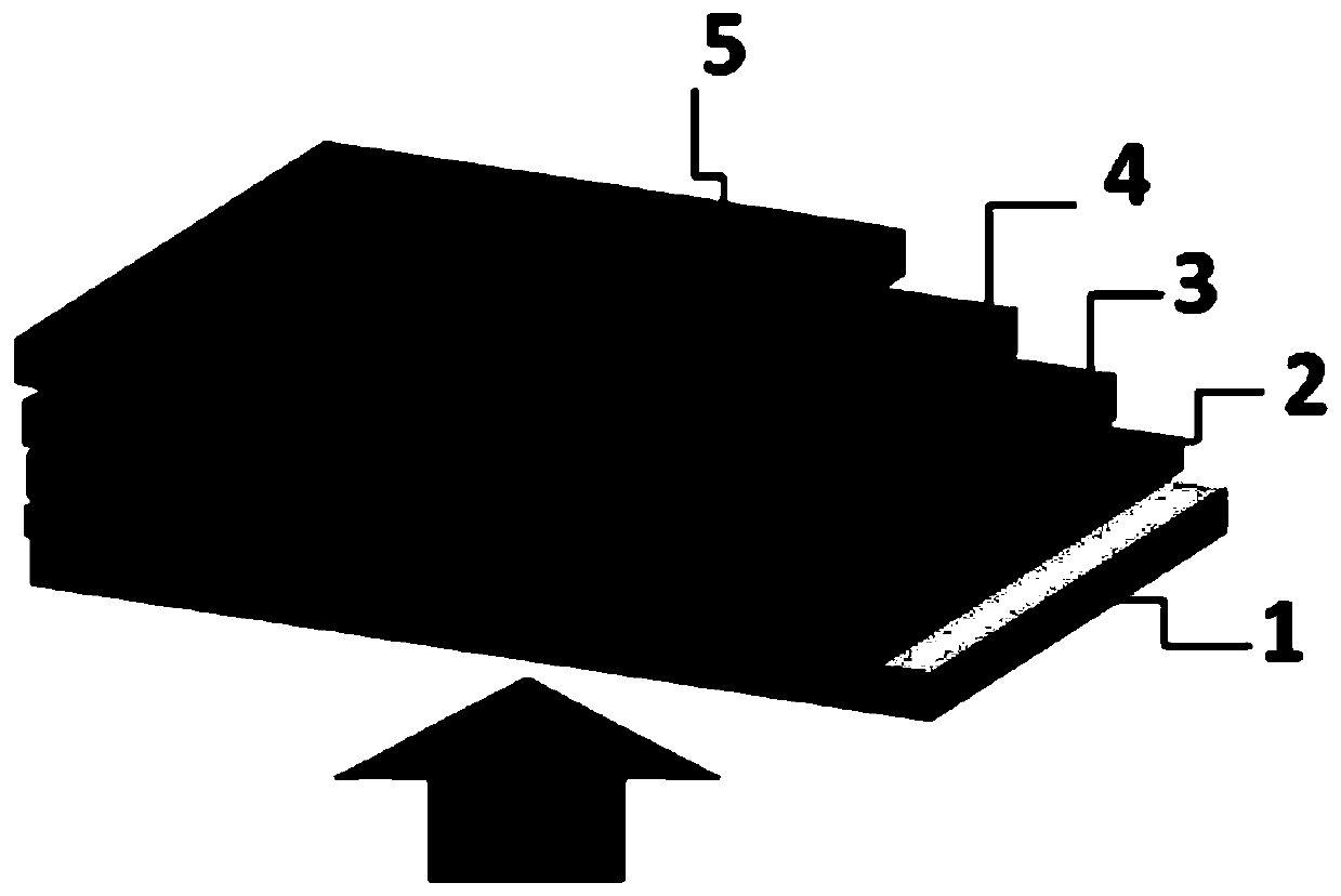
[0049] (1) The commercial FTO was partially etched by the mixed reaction of dilute hydrochloric acid (HCl) and zinc powder (Zn), and then the substrate was ultrasonically cleaned in deionized water, acetone and isopropanol for 15 minutes each; The substrate was blown dry with nitrogen, and treated with ultraviolet ozone for 30 minutes.
[0050] (2) Deposit a layer of aluminum oxide film with a thickness of 1.5nm on the substrate treated by (1) by ALD technology (model: BENEQ, TFS200), the precursor source is trimethylaluminum (TMA), and the deposition conditions are: The chamber temperature was 85° C., the chamber pressure was 9 Pa, and the growth cycle was 16 times.
[0051] (3) Dissolve 0.33mol cesium bromide and 0.33mol lead bromide in 1mL dimethyl sulfoxide solution, heat and stir at 70°C for 12h to obtain CsPbBr 3 Precursor solution: Spin-coat the precursor solution on the aluminum oxide film, the spin-coating conditions are: spin-coating at 500rpm for 6 seconds, and spi...
Embodiment 2
[0056] 1. With reference to Example 1, only the thickness of the aluminum oxide thin film layer in step (2) is made into 1nm by ALD technology, wherein the growth cycle is 11 times, and other process parameters are the same as in Example 1 to obtain an all-inorganic perovskite photoelectric detector. The device has low dark current and high stability.
[0057] 2. With reference to Example 1, only the thickness of the aluminum oxide film layer in step (2) is made into 3nm by ALD technology, wherein the growth cycle is 32 times, and other process parameters are the same as in Example 1 to obtain an all-inorganic perovskite photoelectric detector. The device has low dark current and high stability.
[0058] 3. With reference to Example 1, only the thickness of the titanium oxide film layer in step (4) is made into 5nm by ALD technology, wherein the growth cycle is 86 times, and other process parameters are the same as in Example 1 to obtain an all-inorganic perovskite photoelec...
Embodiment 3
[0061] With reference to Example 1, only the commercial FTO in step (1) is changed into PET / ITO, and other process parameter conditions are the same as in Example 1 to obtain an all-inorganic perovskite photodetector, and its current-time curve is as follows Figure 9 shown.
PUM
| Property | Measurement | Unit |
|---|---|---|
| thickness | aaaaa | aaaaa |
| thickness | aaaaa | aaaaa |
| thickness | aaaaa | aaaaa |
Abstract
Description
Claims
Application Information


