Gallium nitride-based light-emitting diode epitaxial wafer and manufacturing method thereof

A light-emitting diode, gallium nitride-based technology, applied in semiconductor devices, electrical components, circuits, etc., can solve the problems of the deterioration of the crystal quality of the bottom layer of the epitaxial layer, the poor crystal quality of the three-dimensional nucleation layer, and the poor crystal quality of the buffer layer. The effect of preventing excessive beryllium doping, improving crystal quality and increasing the degree of aggregation

Active Publication Date: 2020-10-16
HC SEMITEK ZHEJIANG CO LTD
View PDF7 Cites 0 Cited by
  • Summary
  • Abstract
  • Description
  • Claims
  • Application Information

AI Technical Summary

Problems solved by technology

[0005] The crystal quality of the buffer layer grown in a low temperature environment is poor, which will make the crystal quality of the three-dimensional nucleation layer grown on it poor, resulting in more dislocation density, resulting in a decrease in the crystal quality of the bottom layer of the epitaxial layer, which is difficult to obtain later. The epitaxial layer with better crystal quality seriously affects the quality of LED

Method used


Image

  • Gallium nitride-based light-emitting diode epitaxial wafer and manufacturing method thereof
  • Gallium nitride-based light-emitting diode epitaxial wafer and manufacturing method thereof

Examples


Embodiment Construction

[0026] In order to make the object, technical solution and advantages of the present invention clearer, the implementation manner of the present invention will be further described in detail below in conjunction with the accompanying drawings.

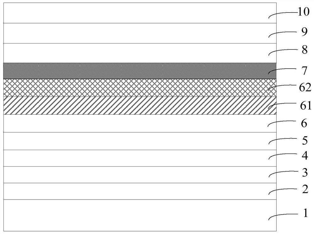
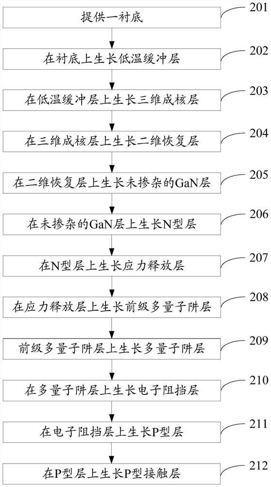
[0027] figure 1 It is a schematic structural diagram of a gallium nitride-based light-emitting diode epitaxial wafer provided by an embodiment of the present invention, as shown in figure 1 As shown, the light-emitting diode epitaxial wafer includes a substrate 1, and a low-temperature buffer layer 2, a three-dimensional nucleation layer 3, a two-dimensional recovery layer 4, an undoped GaN layer 5, and an N-type layer 6 grown on the substrate 1 in sequence. , multi-quantum well layer 7, electron blocking layer 8 and P-type layer 9.

[0028] Both the low-temperature buffer layer 2 and the three-dimensional nucleation layer 3 are beryllium-doped GaN layers. The doping concentration of beryllium in the low-temperature buffer layer 2 inc...


PUM

PropertyMeasurementUnit
thicknessaaaaaaaaaa
thicknessaaaaaaaaaa
pressureaaaaaaaaaa

Abstract

The invention discloses a gallium nitride-based light emitting diode epitaxial wafer and a manufacturing method thereof, and belongs to the technical field of semiconductors. The gallium nitride-basedlight emitting diode epitaxial wafer comprises a substrate, and a low-temperature buffer layer, a three-dimensional nucleating layer, a two-dimensional recovery layer, an undoped GaN layer, an N-typelayer, a multi-quantum well layer, an electron blocking layer and a P-type layer which grow on the substrate in sequence, wherein the low-temperature buffer layer and the three-dimensional nucleatinglayer are both beryllium-doped GaN layers, the doping concentration of beryllium in the low-temperature buffer layer is gradually increased in the stacking direction of the epitaxial wafer, and the doping concentration of beryllium in the three-dimensional nucleating layer is gradually reduced in the stacking direction of the epitaxial wafer. The gallium nitride-based light emitting diode epitaxial wafer provided by the invention can improve the bottom crystal quality of the epitaxial layer, thereby improving the crystal quality of the epitaxial layer.

Description

technical field [0001] The invention relates to the technical field of semiconductors, in particular to a gallium nitride-based light-emitting diode epitaxial wafer and a manufacturing method thereof. Background technique [0002] LED (Light Emitting Diode, Light Emitting Diode) is a semiconductor electronic component that can emit light. As an efficient, environmentally friendly and green new solid-state lighting source, it is being rapidly and widely used, such as traffic lights, car interior and exterior lights, urban landscape lighting, mobile phone backlights, etc. [0003] The epitaxial wafer is the main component of the LED. The existing GaN-based LED epitaxial wafer includes a substrate, a low-temperature buffer layer, a three-dimensional nucleation layer, a two-dimensional recovery layer, and an undoped GaN layer stacked on the substrate in sequence. , N-type layer, multiple quantum well layer, electron blocking layer and P-type layer. Due to the large difference ...

Claims


Application Information

Patent Timeline
Patent Type & Authority Patents(China)
IPC IPC(8): H01L33/00H01L33/02H01L33/12H01L33/32
Inventor 刘旺平乔楠吕蒙普胡加辉李鹏
Owner HC SEMITEK ZHEJIANG CO LTD
Why Eureka
Try Eureka