A preparation method of two-terminal artificial synapse electronic device based on organic/inorganic hybrid perovskite

An electronic device, perovskite technology, applied in the field of artificial synapse electronic devices at both ends, can solve the problem of low sensitivity of artificial synapse, achieve high sensitivity, simplify the process, and reduce manufacturing costs

Active Publication Date: 2020-11-27
NANKAI UNIV
View PDF0 Cites 0 Cited by
  • Summary
  • Abstract
  • Description
  • Claims
  • Application Information

AI Technical Summary

Problems solved by technology

[0004] The purpose of the present invention is to solve the problem that the sensitivity of artificial synapses is generally low at present, and at the same time reduce device energy consumption, save energy, and facilitate future large-scale integration

Method used


Image

  • A preparation method of two-terminal artificial synapse electronic device based on organic/inorganic hybrid perovskite
  • A preparation method of two-terminal artificial synapse electronic device based on organic/inorganic hybrid perovskite
  • A preparation method of two-terminal artificial synapse electronic device based on organic/inorganic hybrid perovskite

Examples


Embodiment 1

[0025] (1) Divide 1.5×1.5cm 2 Put the highly doped silicon substrate into an acetone solution for ultrasonic cleaning for 15 minutes, then put it into an isopropanol (IPA) solution for ultrasonic cleaning for 15 minutes, then heat the IPA to boiling, and fumigate the surface of the substrate with IPA hot steam. then use N 2 Gun to dry its surface.

[0026] (2) Lead bromide (PbBr) with a molar ratio of 1:1 2 ) and methyl ammonium chloride (MACl) are mixed and dissolved in dimethylformamide (DMF) at a volume ratio of 4:1: dimethyl sulfoxide (DMSO) mixed solvent, and then the mixture is placed in a magnetic stirrer Stir until clear and transparent, and configure MAPbClBr with a mass fraction of 20% 2 perovskite solution.

[0027] (3) Place the obtained silicon substrate in an ultraviolet ozone cleaner for 20 minutes, take 50 μL of perovskite solution on the obtained silicon substrate with a pipette gun, -1 Spin coating at 5000r min for 10s, followed by -1 At the same time, ...

Embodiment 2

[0031] (1) Divide 1.5×1.5cm 2 Put the highly doped silicon substrate into an acetone solution for ultrasonic cleaning for 15 minutes, then put it into an isopropanol (IPA) solution for ultrasonic cleaning for 15 minutes, then heat the IPA to boiling, and fumigate the surface of the substrate with IPA hot steam. then use N 2 Gun to dry its surface.

[0032] (2) Lead bromide (PbBr) with a molar ratio of 1.1:1 2 ) and methyl amine bromide (MABr) are mixed and dissolved in dimethylformamide (DMF): dimethyl sulfoxide (DMSO) mixed solvent with a volume ratio of 5:2, and then the mixture is placed in a magnetic stirrer Stir until clear and transparent, and configure MAPbBr with a mass fraction of 20% 3 perovskite solution.

[0033] (3) Place the obtained silicon substrate in an ultraviolet ozone cleaner for 20 minutes, take 50 μL of perovskite solution on the obtained silicon substrate with a pipette gun, -1Spin coating at the speed of 15s, followed by 3500r min -1 At the same ...

Embodiment 3

[0037] (1) Divide 1.5×1.5cm 2 Put the highly doped silicon substrate into an acetone solution for ultrasonic cleaning for 15 minutes, then put it into an isopropanol (IPA) solution for ultrasonic cleaning for 15 minutes, then heat the IPA to boiling, and fumigate the surface of the substrate with IPA hot steam. then use N 2 Gun to dry its surface.

[0038] (2) Lead bromide (PbBr) with a molar ratio of 1:1 2 ) and methyl ammonium chloride (MACl) are mixed and dissolved in dimethylformamide (DMF) at a volume ratio of 4:1: dimethyl sulfoxide (DMSO) mixed solvent, and then the mixture is placed in a magnetic stirrer Stir until clear and transparent, and configure MAPbClBr with a mass fraction of 10% 2 perovskite solution.

[0039] (3) Place the obtained silicon substrate in an ultraviolet ozone cleaner for 20 minutes, take 70 μL of perovskite solution on the obtained silicon substrate with a pipette gun, -1 Spin coating at a speed of 10s, followed by 3000r min -1 At the same...


PUM


Abstract

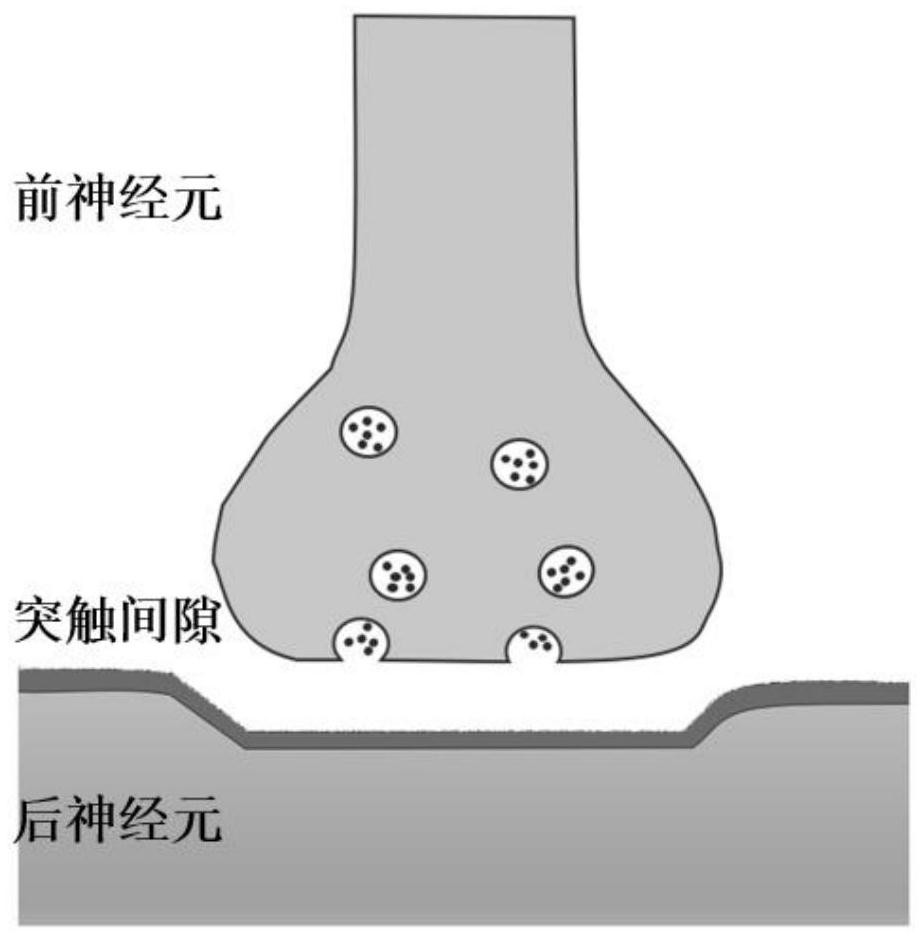
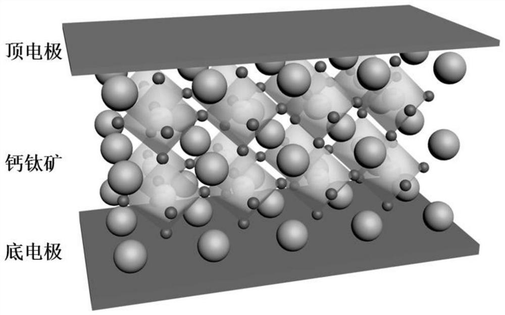
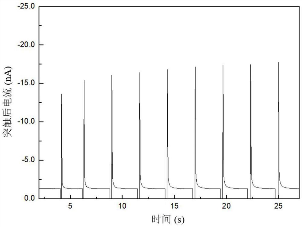
The invention discloses a preparation method of an electronic device with artificial synapsis at two ends based on organic / inorganic hybrid perovskite, and belongs to the field of the electronic device. The preparation method comprises the following steps: pre-treating a high-doped silicon substrate, spinning-coating a configured perovskite solution on a substrate, performing annealing treatment to obtain a perovskite thin film with good crystallinity; and then evaporating a metal top electrode to obtain the electronic device with perovskite artificial synapsis at two ends. Since the top electrode simulates the biological synapsis cephacoria, a perovskite active layer simulates the synaptic cleft, and a bottom electrode simulates synapsis caudacoria, the perovskite artificial synapsis hascomparatively high sensitivity (100mA), and the dual-pulse facilitation, the peak voltage dependence plasticity, peak persistent dependence plasticity and peak frequency dependence plasticity are realized. The preparation method disclosed by the invention not only can effectively simplify the basic structures of the perovskite artificial synapsis at two ends, the sensitivity is improved, the energy consumption is reduced, and the preparation method has significance for the development of the neuromorphic engineering and the human-like robot.

Description

technical field [0001] The invention belongs to the field of electronic devices, in particular to electronic devices with artificial synapses at both ends. Background technique [0002] With the advent of the era of artificial intelligence, neuromorphic engineering (Neuromorphic Engineering), which simulates the structure, function and computing principles of the human brain, is developing rapidly. By simulating complex functions such as memory, calculation, and cognition of the human brain, this artificial neuromorphic system can achieve extremely high computing speed and efficiency, and is expected to break through many limitations of traditional computer chips. Although the computing power of modern computers has been continuously improved with the development of electronics and information technology, their functionality is still not comparable to that of the real human brain. The human brain takes up less than 2 liters of volume and consumes as much energy as a househo...

Claims


Application Information

Patent Timeline
Patent Type & Authority Patents(China)
IPC IPC(8): H01L51/40B82Y10/00B82Y15/00
Inventor 徐文涛于海洋龚江东
Owner NANKAI UNIV
Why Eureka
Try Eureka