Silicon heterojunction/perovskite based double-electrode laminated solar cell

A solar cell and silicon heterojunction technology, applied in the field of solar cells, can solve the problems of restricting cell performance, weak perovskite spectral response, and large band gap

Pending Publication Date: 2019-06-25
PEKING UNIV
View PDF3 Cites 17 Cited by
  • Summary
  • Abstract
  • Description
  • Claims
  • Application Information

AI Technical Summary

Problems solved by technology

However, due to its large band gap, the spectral response of perovskite in the nea

Method used


Image

  • Silicon heterojunction/perovskite based double-electrode laminated solar cell
  • Silicon heterojunction/perovskite based double-electrode laminated solar cell
  • Silicon heterojunction/perovskite based double-electrode laminated solar cell

Examples


Embodiment 1

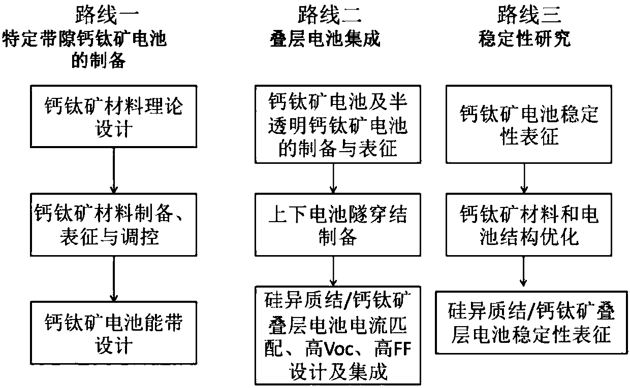
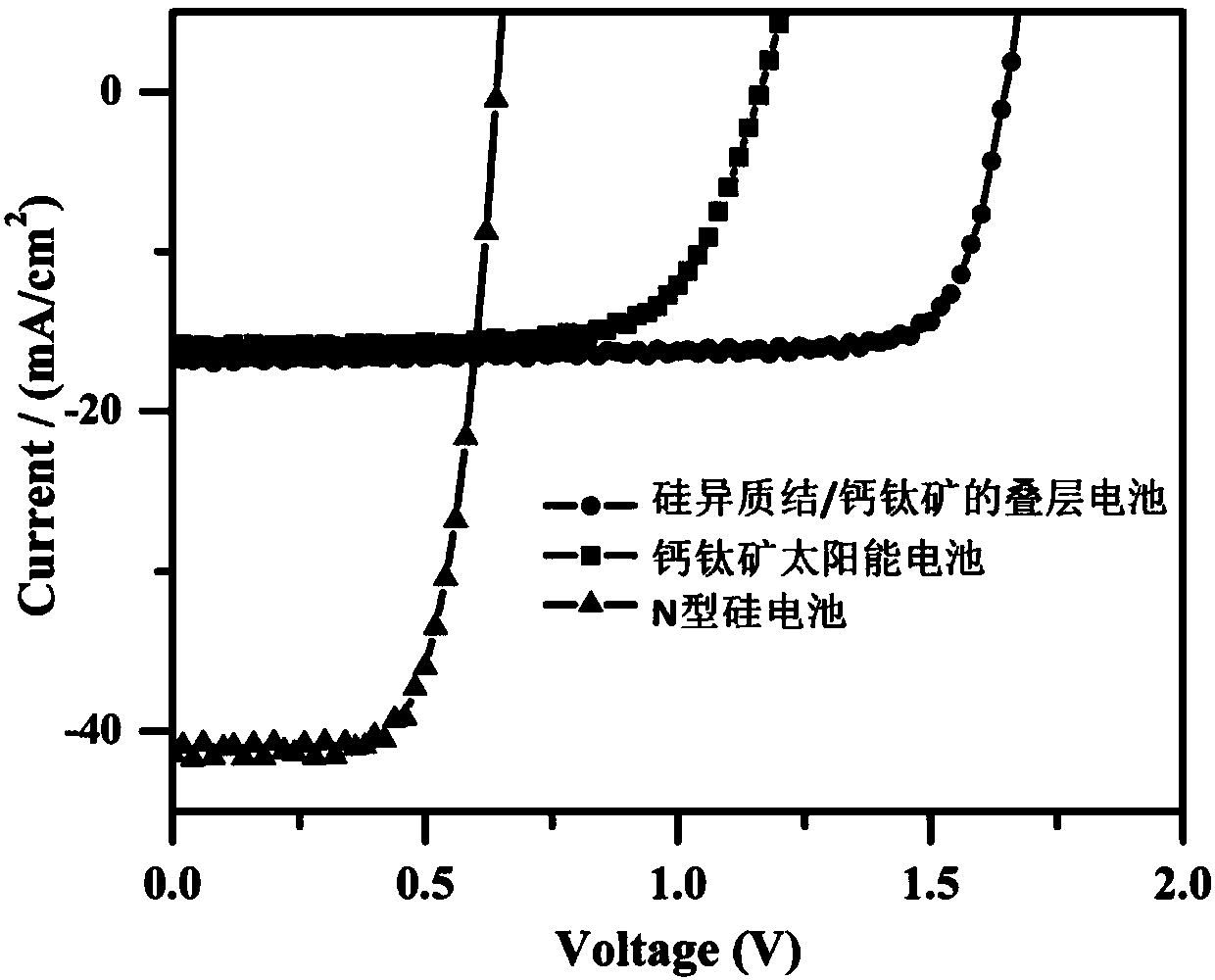
[0030] Embodiment 1 (stack efficiency optimization based on different perovskite bandgap widths)

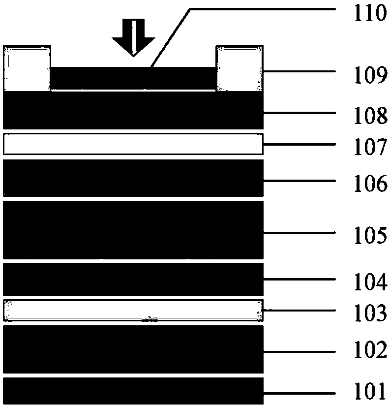
[0031] (1) Commercialized n-type heterojunction Si cells with a size of 1cm*1cm;

[0032] (2) Magnetron sputtering power 80nm ITO film is used as the connecting layer of the upper and lower batteries on the Si battery;

[0033] (3) The Si battery after sputtering is ultrasonicated with ethanol solution for 10 minutes, dried with a nitrogen gun, and then used with a UV cleaning machine for 20 minutes to increase the wettability of the solution and remove organic matter on the surface;

[0034] (4) Preparation of electron transport layer: SnO 2 2H 2 O (purchased from Alfa Aesar) is spin-coated on the Si substrate, spin-coated with a homogenizer at 3000rpm*30s, and then annealed at 150°C for 30min to form dense SnO 2 Thin film; annealed at 3000rpm150℃ for 30min.

[0035] (5) For the preparation of perovskite absorbing layers with different band gaps, first configure the precurso...

Embodiment 2

[0042] Embodiment 2 (optimizing the electron transport layer)

[0043] This embodiment provides a method for preparing a perovskite solar cell. The preparation method provided in this embodiment three is basically the same as that of embodiment one, except that the spin-coated electron transport layer in step (4) of embodiment one is The rotation speed was changed, and then the thickness of the tin dioxide layer was changed, and a composite electron transport layer (composite of titanium dioxide and tin dioxide) was tried, so that the electron transport layer could be used to modify the surface fluctuation of the Si battery to reduce the Its roughness provides a good environment for the growth of the upper layer of perovskite, and improves the extraction efficiency of photogenerated electrons, avoiding the impact of charge accumulation on the life of the device.

[0044] Table 2 Effect of regulation of electron transport layer on device performance

[0045]

Embodiment 3

[0046] Embodiment three (exploring whether magnesium fluoride can improve the efficiency of the battery)

[0047] (1) The etched ITO glass has a size of 1.5cm*1.5cm. The transparent conductive glass is washed and cleaned by the traditional substrate cleaning process.

[0048] (2) After drying with a nitrogen gun, use a UV cleaning machine for 20 minutes to increase the wettability of the solution and remove organic matter on the surface;

[0049] (3) Step (4) with the above-mentioned implementation case one;

[0050] (4) The preparation of the perovskite absorbing layer, first configure the precursor of two-step spin coating, dissolve 230mg lead iodide and 150mg lead bromide in 1ml N, N dimethylformamide (DMF) solvent, 70 °C and stirred for 5 hours. Spread 35ul of the precursor solution on the substrate, spin dry at 3000rpm*30s, and anneal at 70°C for 20min to form a bright yellow film. Dissolve 40mg of methyl iodide and 20 mg of methyl iodide in 1ml of isopropanol, and sti...


PUM

PropertyMeasurementUnit
Thicknessaaaaaaaaaa
Thicknessaaaaaaaaaa
Thicknessaaaaaaaaaa

Abstract

The invention relates to a preparation method for a silicon heterojunction/perovskite based double-electrode laminated solar cell. Compared with a unijunction solar cell, the laminated solar cell canutilize medium-short wave photons in the sun spectrum more effectively to achieve a higher efficiency. The laminated solar cell based on silicon heterojunction/perovskite electrodes comprises a top wide-band-gap perovskite solar cell and a narrow-band-gap silicon cell, and also comprises an anti-reflecting layer, a transparent top electrode, a protective layer, a perovskite absorbing layer, an electron transmission layer, an intermediate layer, a Si heterojunction battery and a metal electrode successively from top to bottom. The tunnel junction and perovskite absorbing layer are prepared at low temperature. The silicon heterojunction/perovskite double-electrode laminated solar cell prepared by a simple low-cost solution method can reach the efficiency of 22.22% which is in a leading position domestically.

Description

technical field [0001] The invention relates to the field of solar cells, in particular to a method for preparing a stacked solar cell based on a silicon heterojunction / perovskite two-electrode. Background technique [0002] The energy distribution of the solar spectrum is relatively wide, and the photoelectric response spectrum range of a single semiconductor material is too narrow compared with the solar spectrum, which fundamentally restricts the improvement of efficiency. Combining semiconductor materials with different bandgap widths to form multi-junction semiconductor solar cells. The incident light of different wavelength ranges is absorbed respectively, and the energy band of the top cell is the largest, and the energy band of the bottom layer decreases successively. Multi-junction semiconductor solar cells have become the most potential solar cells for current applications due to their advantages such as high conversion efficiency, good temperature characteristics...

Claims


Application Information

Patent Timeline
IPC IPC(8): H01L51/42H01L31/0725H01L51/48
CPCY02E10/549Y02B10/10
Inventor 周欢萍邱智文徐梓淇周宁李能旭陈怡华赵冠超李厉伟孟原郭铁
Owner PEKING UNIV
Why Eureka
Try Eureka