A flexible color micro-led preparation method and prepared product
A flexible and colorful technology, applied in the field of flexible color Micro-LED preparation methods and prepared products, can solve the problems of huge number of chips, color conversion, transfer, etc., achieve large transfer volume, reduce production costs, reduce the number of times of transfer and the effect of time
- Summary
- Abstract
- Description
- Claims
- Application Information
AI Technical Summary
Problems solved by technology
Method used
Image
Examples
Embodiment 1
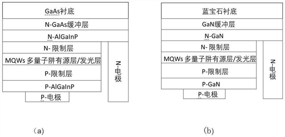
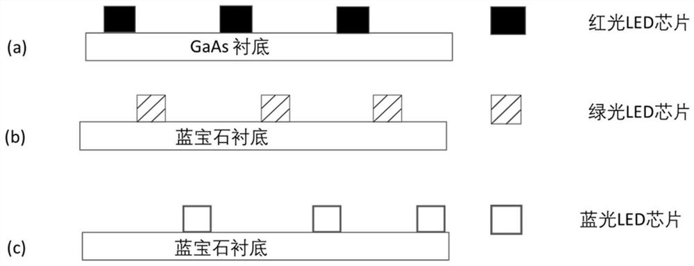
[0026] Step 1. Pre-fabrication of patterned red flip-chip microchips (pixels) on the GaAs substrate LED wafer (including epitaxial layer) by photolithography or mutual induction coupled plasma etching (ICP) (see figure 1 (a)), with a size of 8 μm. Anneal the manufactured Micro-LED chips in a vacuum furnace.
[0027] Step 2. Make patterned GaN-based green and blue flip chips (pixels) on the sapphire substrate LED wafer (including epitaxial layer) by photolithography or inductively coupled plasma etching (ICP) respectively (see figure 1 (b) and (c)), with a size of 8 μm. The green and blue chips produced were annealed in a vacuum furnace respectively.
[0028] Step 3, performing selective etching on the GaAs substrate of the red light microchip to obtain a patterned chip supported by a thin film.
[0029] Step 4, the sapphire substrates on the green light and blue light microchips are respectively lifted off by laser.
[0030] Step 5. Translating the pattern-shaped red light...
Embodiment 2
[0036] Step 1. Pre-fabrication of patterned red flip-chip microchips (pixels) on the GaAs substrate LED wafer (including epitaxial layer) by photolithography or mutual induction coupled plasma etching (ICP) (see figure 1 (a)), with a size of 7 μm. Anneal the manufactured Micro-LED chips in a vacuum furnace.
[0037] Step 2. Make patterned GaN-based green and blue flip chips (pixels) on the sapphire substrate LED wafer (including epitaxial layer) by photolithography or inductively coupled plasma etching (ICP) respectively (see figure 1 (b) and (c)), with a size of 7 μm. The green and blue chips produced were annealed in a vacuum furnace respectively.
[0038] Step 3, performing selective etching on the GaAs substrate of the red light microchip to obtain a patterned chip supported by a thin film.
[0039] Step 4, the sapphire substrates on the green light and blue light microchips are respectively peeled off by laser.
[0040] Step 5. Translating the pattern-shaped red light...
Embodiment 3
[0046] Step 1. Pre-fabrication of patterned red flip-chip microchips (pixels) on the GaAs substrate LED wafer (including epitaxial layer) by photolithography or mutual induction coupled plasma etching (ICP) (see figure 1(a)), with a size of 6 μm. Anneal the manufactured Micro-LED chips in a vacuum furnace.
[0047] Step 2. Make patterned GaN-based green and blue flip chips (pixels) on the sapphire substrate LED wafer (including epitaxial layer) by photolithography or inductively coupled plasma etching (ICP) respectively (see figure 1 (b) and (c)), with a size of 6 μm. The green and blue chips produced were annealed in a vacuum furnace respectively.
[0048] Step 3, performing selective etching on the GaAs substrate of the red light microchip to obtain a patterned chip supported by a thin film.
[0049] Step 4, the sapphire substrates on the green light and blue light microchips are respectively lifted off by laser.
[0050] Step 5. Translating the pattern-shaped red light ...
PUM
| Property | Measurement | Unit |
|---|---|---|
| size | aaaaa | aaaaa |
Abstract
Description
Claims
Application Information


