


Quick Research
Generate reliable direction feasibility study reports for your R&D in just a few steps.

Technical Q&A
Discover and master advanced knowledge NOW. Basics, ideas, possibilities, all at once.

Find Solutions
As an expert in R&D theories, this can generate solutions to your technical problems instantly.

Evaluate Feasibility
Analyze your overall solution with one click, know your potential R&D risks in advance.

Monitor Landscape
Get weekly tech updates, stay abreast of the latest tech innovations and key insights.
MEMS device, preparation method and electronic device
A technology of electronic devices and devices, which is applied in the direction of microelectronic microstructure devices, manufacturing microstructure devices, microstructure devices, etc., can solve the problems of device performance and yield decline, MEMS devices cannot be packaged, and contact pads fall off, etc., to achieve The effect of improving performance and yield
- Summary
- Abstract
- Description
- Claims
- Application Information
AI Technical Summary
Problems solved by technology
Method used
Image

Examples
Embodiment 1
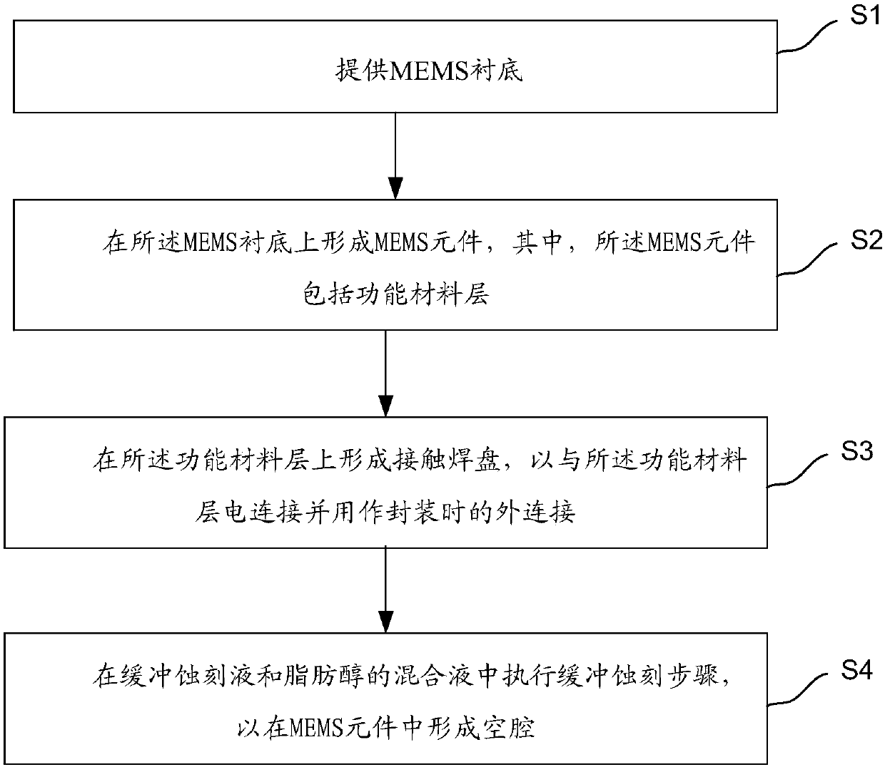
[0054] Reference below figure 2 with Figure 3A-3B The preparation method of the MEMS device of the present invention is described in detail, figure 2 Shows a process flow chart of the preparation of the MEMS device of the present invention; Figure 3A-3B The structure of a MEMS device in an embodiment of the present invention is shown.
[0055] Among them, such as figure 2 As shown, the main steps of the preparation method include:
[0056] Step S1: Provide a MEMS substrate;
[0057] Step S2: forming a MEMS element on the MEMS substrate, wherein the MEMS element includes a functional material layer;
[0058] Step S3: forming contact pads on the functional material layer to be electrically connected to the functional material layer and used as an external connection during packaging;
[0059] Step S4: Perform a buffer etching step in a mixed solution of buffer etching solution and fatty alcohol to form a cavity in the MEMS element.
[0060] Hereinafter, specific implementations of the...
Embodiment 2
[0146] The invention also provides a MEMS device, such as Figure 3B As shown, the MEMS device in the present invention includes:
[0147] MEMS substrate;
[0148] The MEMS element is formed on the MEMS substrate, wherein the MEMS element includes a functional material layer;
[0149] The contact pad is electrically connected to the functional material layer and used as an external connection during packaging.
[0150] The contact pad includes a Cr layer and an Au layer arranged in sequence.
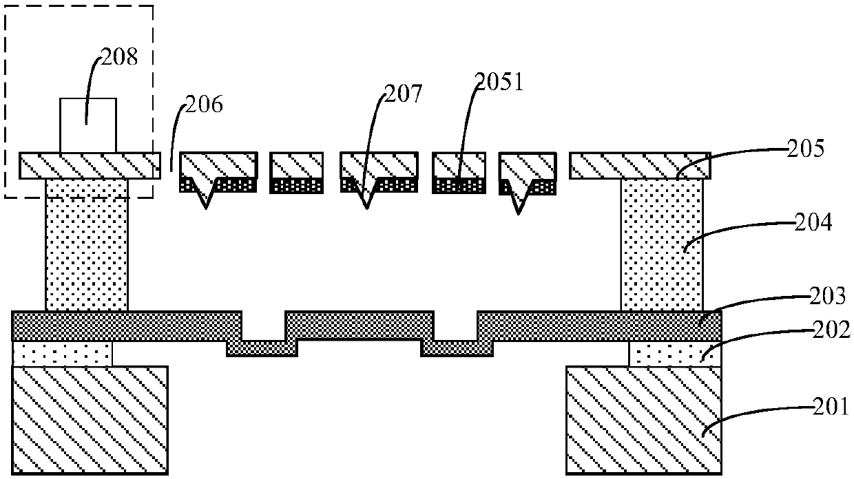
[0151] The MEMS element includes a MEMS microphone, and the MEMS microphone includes:
[0152] Vibrating membrane 303;
[0153] The cavity is located between the vibrating membrane and the back plate;
[0154] Sound holes 306, a number of the sound holes are spaced apart from each other and penetrate the back plate and expose the vibrating membrane;
[0155] The blocking structure 307 is embedded in the surface of the back plate facing the cavity, and the blocking member extends toward the vibrating ...
Embodiment 3
[0173] The present invention also provides an electronic device, which includes the MEMS device described in the second embodiment or the MEMS device prepared by the method described in the first embodiment.
[0174] The electronic device can be any electronic product or equipment such as mobile phone, tablet computer, notebook computer, netbook, game console, TV, VCD, DVD, navigator, camera, camcorder, voice recorder, MP3, MP4, PSP, etc., or It is an intermediate product with the above-mentioned MEMS devices, such as a mobile phone motherboard with the integrated circuit.
[0175] Since the included MEMS device has higher performance, the electronic device also has the above advantages.
[0176] among them, Figure 4 An example of a mobile phone handset is shown. The mobile phone handset 400 is provided with a display portion 402 included in a housing 401, operation buttons 403, an external connection port 404, a speaker 405, a microphone 406, and the like.
[0177] The electronic d...
PUM
| Property | Measurement | Unit |
|---|---|---|
| thickness | aaaaa | aaaaa |
| thickness | aaaaa | aaaaa |
| thickness | aaaaa | aaaaa |
Abstract
Description
Claims
Application Information
 - R&D Engineer
- R&D Manager
- IP Professional
- Industry Leading Data Capabilities
- Powerful AI technology
- Patent DNA Extraction
Browse by: Latest US Patents, China's latest patents, Technical Efficacy Thesaurus, Application Domain, Technology Topic, Popular Technical Reports.
© 2024 PatSnap. All rights reserved.Legal|Privacy policy|Modern Slavery Act Transparency Statement|Sitemap|About US| Contact US: help@patsnap.com