
Wet etching method for nitride materials

A wet etching and nitride technology, applied in electrical components, semiconductor/solid-state device manufacturing, circuits, etc., can solve the problems of slow etching speed, device damage, and no wet etching of GaN, etc. The effect of fast corrosion rate and smooth surface

Inactive Publication Date: 2019-07-12
INST OF SEMICONDUCTORS - CHINESE ACAD OF SCI
View PDF2 Cites 0 Cited by
  • Summary
  • Abstract
  • Description
  • Claims
  • Application Information

AI Technical Summary

Problems solved by technology

Unlike Si materials, GaN materials have a wide band gap and stable chemical and physical properties, making their wet etching process difficult, so far, the dry etching process is used to etch GaN , have not found a suitable wet etching method for GaN
However, this dry etching process can seriously damage the device, while the etching speed of the GaN wet etching process is very slow, so it is very important to find a suitable wet process technology for rapid nitride etching

Method used


Image

  • Wet etching method for nitride materials
  • Wet etching method for nitride materials
  • Wet etching method for nitride materials

Examples


Embodiment 1

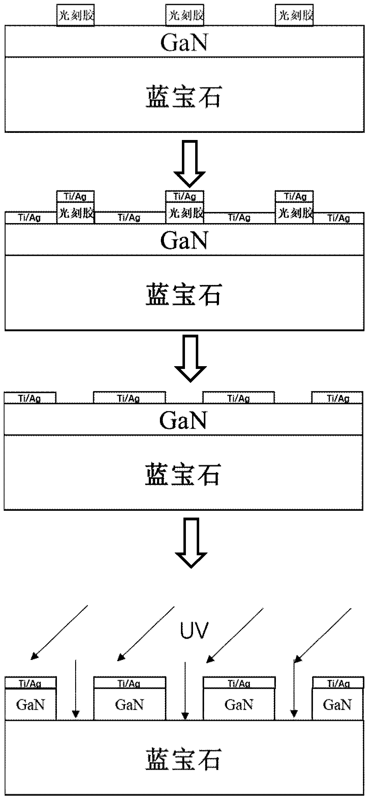
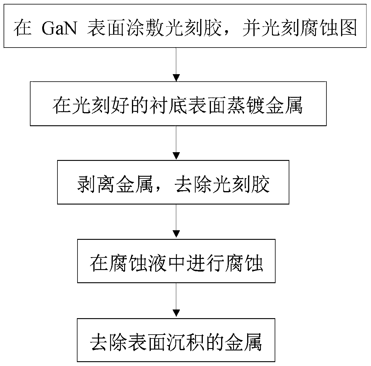
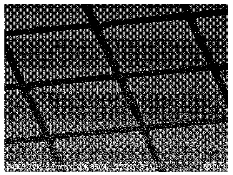
[0042] see figure 2 , and see in conjunction with figure 1 As shown, the substrate used in this embodiment is a sapphire substrate, which was cleaned by the RCA standard cleaning method, and the GaN layer obtained by epitaxy on the sapphire substrate, with a thickness of 6 μm, was cleaned by the RCA standard cleaning method. The GaN substrate was subjected to negative resist photolithography to obtain a square array with a width of 50 μm and a pitch of 5 μm, and then electron beam evaporation was used to vapor-deposit metal Ti / Ag with a thickness of 100 nm and 300 nm on the square array obtained after photolithography, and then Carry out the stripping of the metal with the blue film, expose the part to be corroded, and clean the stripped substrate, remove the photoresist on the surface of the substrate, and then clean it with deionized water. Configure CuSO 4 and HF mixed solution as corrosion solution, CuSO 4 The concentration of the solution is set to 0.015mol / L, and the...


PUM


Abstract

The invention relates to a wet etching method for isotropically etching nitride materials. The method comprises the steps of: coating a photoresist on the surface of GaN, and photoetching and etchinga pattern; evaporating a layer of metal on the photoetching substrate; performing metal stripping, and removing the residual photoresist; then putting the treated GaN into corrosive solution for corrosion; and finally, immersing the etched epitaxial wafer sample into a diluted nitric acid solution to remove surface metal. The method is high in etching speed, low in etching cost and simple in process, and the surface of the etched GaN is flat, the etched pattern can be automatically regulated and controlled according to the requirement.

Description

technical field [0001] The invention relates to the field of wet etching technology for semiconductor materials, in particular to a wet etching method for nitride materials. Background technique [0002] Gallium nitride material (GaN) is widely used in high-power optoelectronic devices due to its excellent properties such as wide band gap, high breakdown voltage, and high electron saturation velocity. Etching is a critical step in the fabrication of GaN devices, and the etching process has received more and more attention. Unlike Si materials, GaN materials have a wide band gap and stable chemical and physical properties, making their wet etching process difficult, so far, the dry etching process is used to etch GaN , have not yet found a suitable wet etching method for GaN. However, this dry etching process seriously damages the device, while the etching speed of the GaN wet etching process is very slow, so it is very important to find a suitable wet process technology fo...

Claims


Application Information

Patent Timeline
IPC IPC(8): H01L21/306H01L21/308
CPCH01L21/30604H01L21/308
Inventor 袁国栋王琦赵帅刘文强王军喜李晋闽
Owner INST OF SEMICONDUCTORS - CHINESE ACAD OF SCI
Learn More