Manufacturing method and application of embedded metal grid flexible transparent electrode

A metal grid and transparent electrode technology, which is applied in cable/conductor manufacturing, additive manufacturing, equipment for manufacturing conductive/semiconductive layers, etc., can solve the limitations of embedded metal grid materials, difficulty in demoulding, falling off or peeling off and other issues, to achieve the effects of efficient continuous production, low production process cost, and widening types and types

Active Publication Date: 2019-07-16
QINGDAO TECHNOLOGICAL UNIVERSITY +1
View PDF6 Cites 21 Cited by
  • Summary
  • Abstract
  • Description
  • Claims
  • Application Information

AI Technical Summary

Problems solved by technology

However, there are many defects and deficiencies in this kind of flexible transparent electrode with metal mesh attached to the surface of the transparent substrate: (1) The surface is poor in flatness, which is easy to cause defects such as short circuit
Since the metal grid transparent electrode is on the surface of the transparent substrate, the surface of the flexible transparent electrode is uneven and not smooth (the metal grid has a certain thickness), which is easy to cause defects such as short circuits in optoelectronic devices (OLED, organic photovoltaic, etc.), and cause Difficult problems in fabrication of subsequent structures (deposition, sputtering, etc.)
(2) The adhesion between the metal grid and the substrate is poor, the bonding force is small, and it is easy to fall off, especially in the application field that requires frequent bending, which can easily cause partial and overall separation (falling off or peeling) of the metal grid and the substrate. , resulting in product or device failure
(3) The square resistance of the metal grid is large and the electrical performance is poor
It is difficult to realize the manufacture of metal mesh structures with large aspect ratios, especially as the line width decreases below the submicron scale, which makes it difficult to further reduce the square resistance, which seriously affects and restricts the electrical performance
(4) There is Murray interference, which seriously affects the optical performance
[0005] However, the existing processes and technologies face great challenges in manufacturing embedded metal grid flexible transparent electrodes, and it is difficult to realize large-scale embedded metal grid flexible transparent electrodes with high efficiency and low cost.
For example, through photolithography, etching, deposition (electroforming, chemical plating, etc.) , It is especially difficult to realize the fabrication of large-area embedded metal grid flexible transparent electrodes
There are problems in the manufacture of flexible transparent electrodes with embedded metal grids by combining thermal embossing and scrape coating processes: high manufacturing costs, many processes, and it is difficult to realize the manufacture of large-aspect-ratio metal grid structures (for large-area and high-aspect-ratio structures Difficult to release the mold during imprinting, which can easily lead to damage to the mold and imprinted features)
In addition, these two methods also have the following deficiencies and limitations: (1) The materials for embedding metal grids are greatly limited. The sintering temperature cannot be higher than the temperature of the transparent substrate
Most of the existing transparent substrate materials have very poor high temperature resistance. For example, PET sheets generally cannot be higher than 100°C, and PC cannot be higher than 150°C. Therefore, the existing process can only use low-temperature sintering conductive materials
(2) The post-conduction treatment takes a long time and the production efficiency is low (conductive ink is embedded in the embossed groove)
(3) Especially the solvent of the conductive material embedded in the microgroove of the transparent substrate is difficult to completely remove (poor electrical conductivity, large square resistance), seriously affecting its electrical properties

Method used


Image

  • Manufacturing method and application of embedded metal grid flexible transparent electrode
  • Manufacturing method and application of embedded metal grid flexible transparent electrode
  • Manufacturing method and application of embedded metal grid flexible transparent electrode

Examples


Embodiment 1

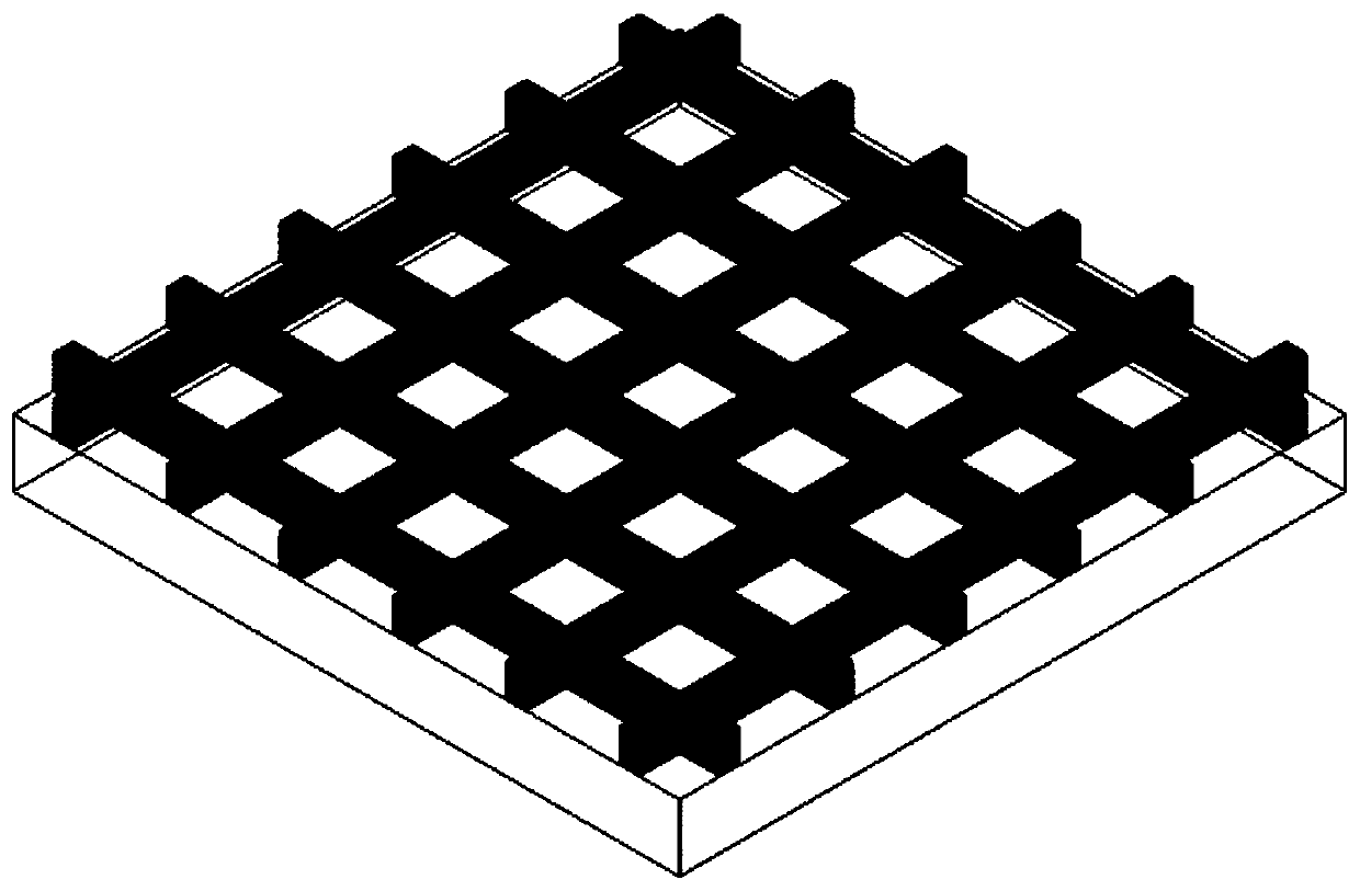
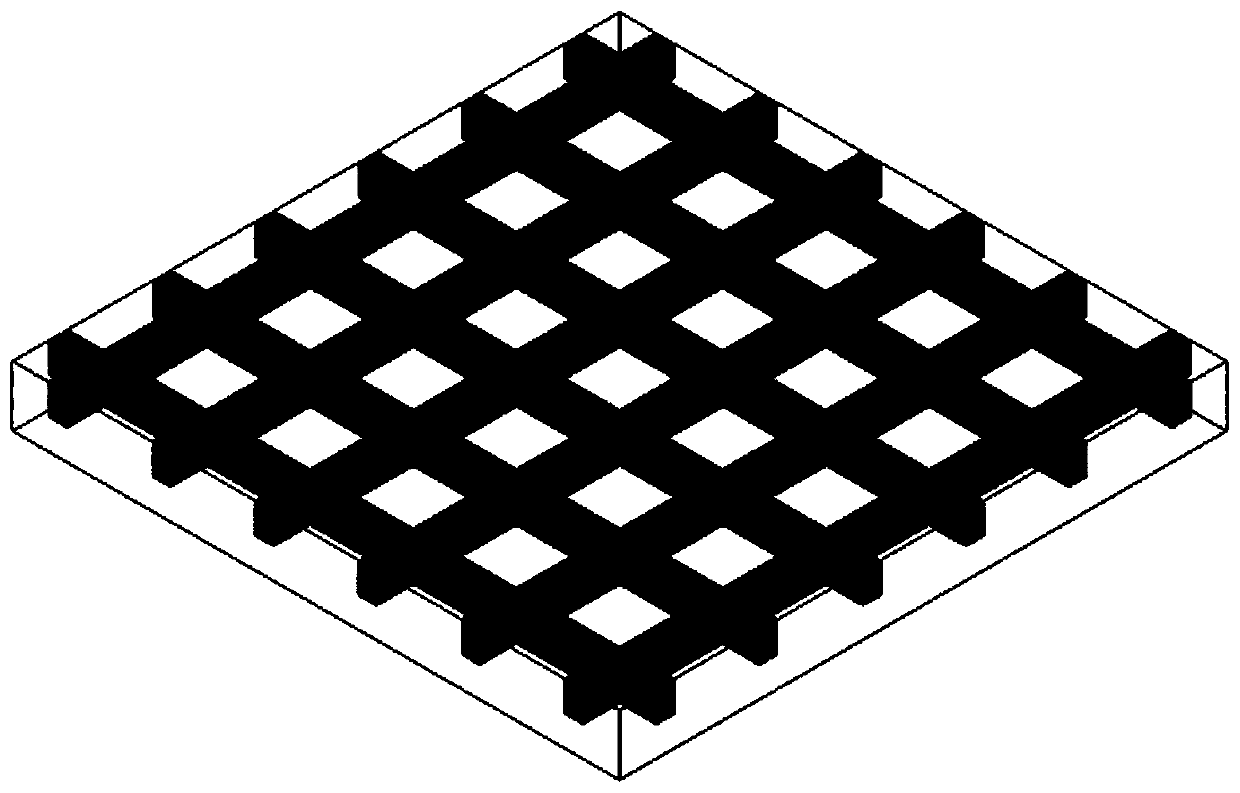
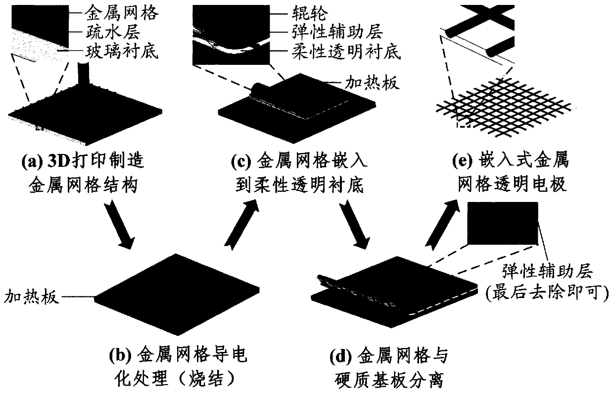
[0049] refer to Figure 2-4 , a method for manufacturing an embedded metal grid flexible transparent electrode, comprising the steps of:

[0050] Step 1: Using electric field-driven spray deposition micro-nano 3D printing to manufacture large-area metal grid structures:

[0051] (1) Take an ordinary glass sheet as the substrate / substrate, after cleaning and drying it, apply a PDMS film on its surface by spin coating with a thickness of 10 μm, and cure the PDMS liquid in a heating environment of 80 °C After 20 minutes, the PDMS was formed into a film to form a hydrophobic layer to obtain a printed substrate. Among them, the hydrophobic layer can reduce the adhesion between the printed metal grid and the substrate, and facilitate the subsequent separation of the metal grid embedded in the flexible transparent substrate from the substrate. At the same time, the hydrophobic layer can increase the aspect ratio of the printed metal grid. It is convenient to improve the light trans...

Embodiment 2

[0059] refer to Figure 2-4 , a method for manufacturing an embedded metal grid flexible transparent electrode, comprising the steps of:

[0060] Step 1: Use micro-nano 3D printing to manufacture a large-area metal grid structure:

[0061] (1) Take an 8-inch silicon wafer as the substrate / substrate, clean it, and then soak it in a solution of heptadecafluorodecyltrichlorosilane + isooctane for 10 minutes to form a self-assembled film (hydrophobic layer) with a thickness of about 200nm. The printed substrate is obtained, wherein the hydrophobic layer can reduce the adhesion between the printed metal grid and the substrate, and facilitate the subsequent separation of the metal grid embedded in the flexible transparent substrate from the substrate. At the same time, the hydrophobic layer can improve the adhesion of the printed metal grid. The aspect ratio is convenient to improve the light transmittance of the subsequent embedded metal grid. The PDMS liquid used is Sylgard 184 ...

Embodiment 3

[0069] refer to Figure 2-4 , a method for manufacturing an embedded metal grid flexible transparent electrode, comprising the steps of:

[0070] Step 1: Using electric field-driven spray deposition micro-nano 3D printing to manufacture large-area metal grid structures:

[0071] (1) Take an ordinary glass sheet as the substrate / substrate, after cleaning and drying it, apply a PDMS film on its surface by spin coating with a thickness of 50 μm, and cure the PDMS liquid in a heating environment of 80 °C After 20 minutes, the PDMS was formed into a film to form a hydrophobic layer to obtain a printed substrate. Among them, the hydrophobic layer can reduce the adhesion between the printed metal grid and the substrate, and facilitate the subsequent separation of the metal grid embedded in the flexible transparent substrate from the substrate. At the same time, the hydrophobic layer can increase the aspect ratio of the printed metal grid. It is convenient to improve the light transmi...


PUM

PropertyMeasurementUnit
thicknessaaaaaaaaaa
thicknessaaaaaaaaaa

Abstract

The invention belongs to the field of flexible transparent electrodes, and particularly relates to a manufacturing method and an application of an embedded metal grid flexible transparent electrode. The method comprises the following steps: 1) by use of an electric field driven spray deposition micro-nano 3D printing technology, a metal grid transparent electrode is directly printed on a hard substrate; 2) conductive treatment is carried out on a printed metal grid structure by adopting a sintering process so as to realize conductive treatment of a metal grid; 3) a flexible transparent substrate and the hard substrate are heated to a set temperature, and a hot stamping process is adopted for completely embedding the metal grid structure on the hard substrate into the flexible transparent substrate; and 4) the metal grid which is completely embedded into the flexible transparent substrate is separated from the hard substrate to obtain the embedded metal grid flexible transparent electrode. According to the method, the electric field driven spray deposition micro-nano 3D printing technology is combined with the roller pair plane hot stamping technology to realize efficient and low-cost batch manufacturing of the large-sized embedded metal grid flexible transparent electrode; and the prepared transparent electrode also has excellent square resistance and light transmittance.

Description

technical field [0001] The invention belongs to the field of flexible transparent electrodes and transparent conductive films, and in particular relates to a high-efficiency and low-cost manufacturing method for embedded metal grid flexible transparent electrodes by combining electric field-driven jet deposition micro-nano 3D printing and thermal embossing. Background technique [0002] The information disclosed in the Background of the Invention is only intended to increase the understanding of the general background of the invention, and it is not necessarily to be taken as an acknowledgment or any form of suggestion that the information constitutes the prior art that is already known to those skilled in the art. [0003] Flexible transparent electrodes / flexible transparent conductive films have a very wide range of applications in many fields such as touch screens, OLEDs, transparent displays, wearable devices, transparent electric heating, transparent antennas, EMI shield...

Claims


Application Information

Patent Timeline
Patent Type & Authority Applications(China)
IPC IPC(8): H01B13/00H01B5/14
CPCH01B13/0026H01B5/14H01B13/0013B33Y80/00B22F10/10B22F10/64B22F2998/10B22F5/10Y02P10/25Y02E10/549B22F10/66B33Y10/00B33Y40/20B22F2301/10B22F2301/255H01B5/16H01B13/0016
Inventor 兰红波刘明杨朱晓阳许权赵佳伟
Owner QINGDAO TECHNOLOGICAL UNIVERSITY
Why Eureka
Try Eureka