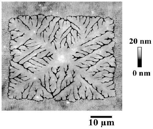
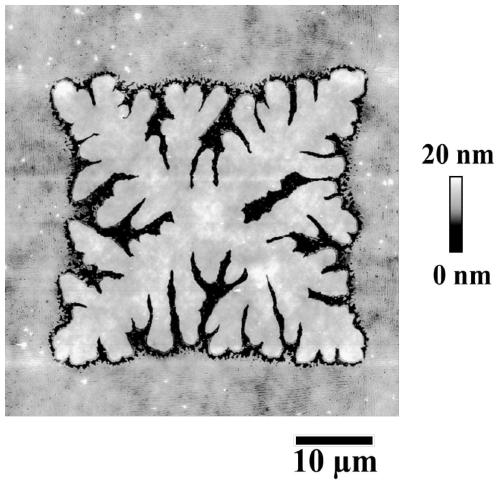
Method for constructing micro-nano patterns in high-molecule film lamellas through selective dissolution
A polymer film and micro-nano pattern technology, applied in the field of polymer micro-nano material processing, can solve the problem of few researches on the lamellar micro-nano structure of the polymer film system
- Summary
- Abstract
- Description
- Claims
- Application Information
AI Technical Summary
Problems solved by technology
Method used
Image
Examples
Embodiment 1
[0061] A method for constructing micro-nano patterns inside polymer thin film lamellar crystals by selective dissolution, the method comprising the following steps:
[0062] (1) Preparation of PEO solution:
[0063] Use acetonitrile as a solvent to dissolve polyethylene oxide with a number average molecular weight of 4.6Kg / mol, then heat on a hot stage to 70°C for 1 hour to completely dissolve PEO in acetonitrile, and configure the mass fraction of PEO in the resulting solution to be 3wt %; then using acetonitrile to dilute the prepared solution to a mass fraction of PEO of 0.3wt%;
[0064] (2) Preparation of PEO film:
[0065] Take the P111 type silicon wafer and irradiate the oxidation treatment with ultraviolet light for 1 hour. After the treatment is completed, place the silicon wafer on a spin coater, and evenly drop the PEO acetonitrile solution (0.01~0.04g) diluted in step (1) on the silicon wafer. Then spin-coat at 4000rpm for 30s, and obtain a polyethylene oxide fil...
Embodiment 2
[0074] A method for constructing micro-nano patterns inside polymer thin film lamellar crystals by selective dissolution, the method comprising the following steps:
[0075] (1) Preparation of PEO solution:
[0076] Use acetonitrile as a solvent to dissolve polyethylene oxide with a number average molecular weight of 4.6Kg / mol, then heat on a hot stage to 70°C for 1 hour to completely dissolve PEO in acetonitrile, and configure the mass fraction of PEO in the resulting solution to be 3wt %; then using acetonitrile to dilute the prepared solution to a mass fraction of PEO of 0.3wt%;
[0077] (2) Preparation of PEO film:
[0078] Take the P111 type silicon wafer and irradiate the oxidation treatment with ultraviolet light for 1 hour. After the treatment is completed, place the silicon wafer on a spin coater, and evenly drop the PEO acetonitrile solution (0.01~0.04g) diluted in step (1) on the silicon wafer. Then spin-coat at 4000rpm for 30s, and obtain a polyethylene oxide fil...
Embodiment 3
[0087] A method for constructing micro-nano patterns inside polymer thin film lamellar crystals by selective dissolution, the method comprising the following steps:
[0088] (1) Preparation of PEO solution:
[0089] Use acetonitrile as a solvent to dissolve polyethylene oxide with a number average molecular weight of 4.6Kg / mol, then heat on a hot stage to 70°C for 1 hour to completely dissolve PEO in acetonitrile, and configure the mass fraction of PEO in the resulting solution to be 3wt %; then using acetonitrile to dilute the prepared solution to a mass fraction of PEO of 0.3wt%;
[0090] (2) Preparation of PEO film:
[0091] Take the P111 type silicon wafer and irradiate the oxidation treatment with ultraviolet light for 1 hour. After the treatment is completed, place the silicon wafer on a spin coater, and evenly drop the PEO acetonitrile solution (0.01~0.04g) diluted in step (1) on the silicon wafer. Then spin-coat at 4000rpm for 30s, and obtain a polyethylene oxide fil...
PUM
 Abstract
Description
Claims
Application Information


