Supercharge Your Innovation With Domain-Expert AI Agents!

A kind of algan ultraviolet avalanche photodiode detector and preparation method thereof

A photodiode, ultraviolet avalanche technology, applied in circuits, electrical components, semiconductor devices, etc., can solve the problem of difficulty in realizing a single carrier avalanche multiplication, and achieve a simple and feasible preparation method, enhanced reliability, and increased electric field strength. Effect

Active Publication Date: 2020-12-22
SUN YAT SEN UNIV
View PDF10 Cites 0 Cited by
  • Summary
  • Abstract
  • Description
  • Claims
  • Application Information

AI Technical Summary

Problems solved by technology

However, in practical devices, it is still difficult for SAM structure APDs to achieve pure single carrier avalanche multiplication.

Method used


Image

  • A kind of algan ultraviolet avalanche photodiode detector and preparation method thereof
  • A kind of algan ultraviolet avalanche photodiode detector and preparation method thereof
  • A kind of algan ultraviolet avalanche photodiode detector and preparation method thereof

Examples


Embodiment 1

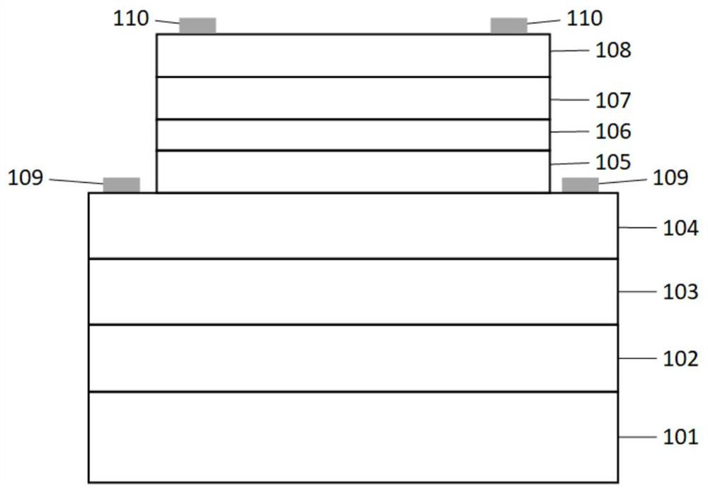
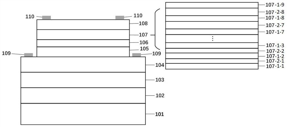
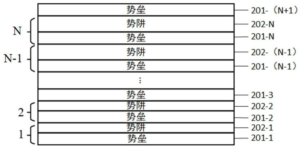
[0041] like figure 1 , figure 2 As shown, an AlGaN ultraviolet avalanche photodiode detector provided in this embodiment includes a sapphire substrate 101 and an epitaxial structure grown on the substrate; the epitaxial structure is an i-type AlN buffer layer 102, i-Al 0.6 Ga 0.4 N transition layer 103, n-type Al 0.6 Ga 0.4 N ohmic contact layer 104, i-type Al 0.4 Ga 0.6 N absorption layer 105, n-type Al 0.4 Ga 0.6 N charge layer 106, i-type Al 0.4 Ga 0.6 N / Al 0.55 Ga 0.45 N superlattice multiplication layer 107, p-type Al 0.4 Ga 0.6 N ohmic contact layer 108; the photodiode detector also includes an ohmic contact electrode, and the ohmic contact electrode includes the n-type Al 0.6 Ga 0.4 The n-type ohmic contact electrode 109 drawn from the N ohmic contact layer 104 and the p-type Al 0.4 Ga 0.6 The p-type ohmic contact electrode 110 drawn on the N ohmic contact layer 108; as image 3 , Figure 4 As shown, the i-type Al 0.4 Ga 0.6 N / Al 0.55 Ga 0.45 The...

Embodiment 2

[0061] A kind of AlGaN ultraviolet avalanche photodiode detector that present embodiment provides, comprises sapphire substrate (101), the epitaxial structure that grows on the substrate; Described epitaxial structure is i-type AlN buffer layer 102, i successively from substrate up Type Al 0.5 Ga 05 N transition layer 103, n-type Al 0.5 Ga 0.5 N ohmic contact layer 104, i-type Al 0.3 Ga 0.7 N absorption layer 105, n-type Al 0.3 Ga 0.7 N charge layer 106, i-type Al 0.3 Ga 0.7 N / Al 0.5 Ga 0.5 N superlattice multiplication layer 107, p-type Al 0.3 Ga 0.7 N ohmic contact layer 108; the photodiode detector also includes an ohmic contact electrode, and the ohmic contact electrode includes the n-type Al 0.5 Ga 0.5 The n-type ohmic contact electrode 109 drawn from the N ohmic contact layer 104 and the p-type Al 0.3 Ga 0.7 The p-type ohmic contact electrode 110 drawn on the N ohmic contact layer 108; the i-type Al 0.3 Ga 0.7 N / Al 0.5 Ga 0.5 The N superlattice multipl...


PUM

PropertyMeasurementUnit
thicknessaaaaaaaaaa
thicknessaaaaaaaaaa
thicknessaaaaaaaaaa

Abstract

The invention provides an AlGaN ultraviolet avalanche photodiode detector. The AlGaN ultraviolet avalanche photodiode detector comprises a substrate and an epitaxial structure, wherein the epitaxial structure is grown on the substrate and comprises an i-type Al<m>Ga<1-M>N / Al<n>Ga<1-N> superlattice multiplication layer, the i-type Al<m>Ga<1-M>N / Al<n>Ga<1-N> superlattice multiplication layer is of agradient well thick structure and is formed by circularly and alternatively arranging relatively low-Al constituent Al<m>Ga<1-m>N well layers and relatively high-Al constituent Al<n>Ga<1-n>N barrierlayers, the thicknesses of the Al<n>Ga<1-n>N barrier layers are maintained unchanged, and the thicknesses of the Al<m>Ga<1-m>N well layers are gradually increased from a substrate side to top. The AlGaN ultraviolet avalanche photodiode detector has the beneficial effects that higher gain can be obtained, excessive noise is favorably prevented, the avalanche working voltage is reduced, and the reliability during working of the device is improved; and meanwhile, the invention also provides a fabrication method of the photodiode detector, and the fabrication method is simple and practical.

Description

technical field [0001] The invention relates to the technical field of group III nitride semiconductor ultraviolet photodetectors, and more specifically relates to an AlGaN ultraviolet avalanche photodiode detector and a preparation method thereof. Background technique [0002] The wavelength of ultraviolet light on the earth is distributed in 10-400nm. The sun is the most important source of natural ultraviolet radiation. Among them, the ultraviolet radiation with a wavelength of 200-280nm is strongly absorbed by the ozone in the earth's stratosphere, and it is difficult to reach the ground through the atmosphere. It is defined as For the sun blind spot. Due to the absorption effect of the atmosphere, ultraviolet detection, especially solar blind detection, has the natural advantage of low background noise. But at the same time, ultraviolet detection also has the disadvantage of weak signal. For a long time, mainstream ultraviolet detectors mostly use ultraviolet photomul...

Claims


Application Information

Patent Timeline
Patent Type & Authority Patents(China)
IPC IPC(8): H01L31/0304H01L31/0352H01L31/107H01L31/18
CPCH01L31/03048H01L31/035236H01L31/1075H01L31/1848
Inventor 江灏颜欢邱新嘉
Owner SUN YAT SEN UNIV
Features
  • R&D
  • Intellectual Property
  • Life Sciences
  • Materials
  • Tech Scout
  • Unparalleled Data Quality
  • Higher Quality Content
  • 60% Fewer Hallucinations
Learn More