N type boron carbon nitrogen film/P type single crystal silicon heresy PN native device and preparation method

A boron carbon nitride, pn junction technology, applied in the field of n-type boron carbon nitride film/p-type single crystal silicon hetero pn junction prototype device and preparation, can solve the limitation of boron carbon nitrogen film research and application development, boron carbon nitrogen film The structural uncertainty of nitrogen films and the difficulty of synthesizing boron carbonitride compounds have achieved the effects of easy industrialization, low cost, high breakdown voltage and working voltage.

Active Publication Date: 2020-08-18
JILIN UNIV
View PDF3 Cites 0 Cited by
  • Summary
  • Abstract
  • Description
  • Claims
  • Application Information

AI Technical Summary

Problems solved by technology

At present, many synthesis methods of boron, carbon and nitrogen cannot determine the composition of boron, carbon and nitrogen, which leads to uncertainty in the structure of boron, carbon and nitrogen films, and hinders the further application of boron, carbon and nitrogen materials.
At the same time, boron carbon nitrogen films are very prone to phase separation of boron nitride and carbon under certain conditions, which makes the synthesis of boron carbon nitrogen compounds very difficult, limiting the research on the properties of boron carbon nitrogen films and the development of applications

Method used


Image

  • N type boron carbon nitrogen film/P type single crystal silicon heresy PN native device and preparation method
  • N type boron carbon nitrogen film/P type single crystal silicon heresy PN native device and preparation method
  • N type boron carbon nitrogen film/P type single crystal silicon heresy PN native device and preparation method

Examples


Embodiment

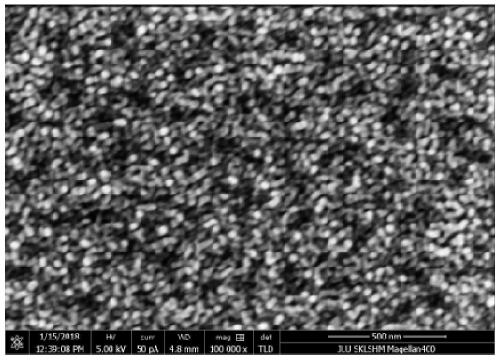
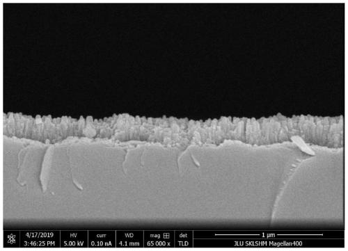
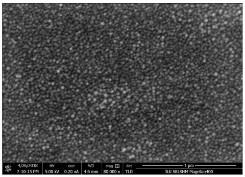
[0029] After the p-type silicon (100) single wafer cut according to the required size is ultrasonically cleaned in acetone, ethanol, and deionized water, it is blown dry with nitrogen and sent to the vacuum deposition chamber. The distance between the substrate and the target is 8cm. The indoor vacuum is pumped to 3×10 - 5 Pa, heat the substrate to 500°C; continue vacuuming until the back vacuum of the deposition chamber reaches 3×10 -5 At Pa, the working gas argon 50sccm is introduced until the working pressure is 2Pa; the base negative bias is applied to -100V, and the target sputtering power is set to 150W to start glowing. After 2 minutes of pre-sputtering, the baffle is removed to perform thin film sputtering. The film sputtering time is 2 hours, and the n-type boron carbon nitrogen film / p-type single crystal silicon heterogeneous pn junction is obtained. Prepare silver electrodes on both sides of the n-type boron carbon nitrogen film / p-type single crystal silicon heter...


PUM

PropertyMeasurementUnit
thicknessaaaaaaaaaa
thicknessaaaaaaaaaa

Abstract

The invention provides an n-type boron carbon nitride thin film / p-type single-crystal heterojunction pn-junction prototype device and a fabrication method thereof, and belongs to the field of semiconductor materials. The fabrication method comprises the steps of fabricating an n-type boron carbon nitride thin film on a p-type (100) surface single-crystal silicon substrate by a magnetron sputteringmethod; and respectively fabricating silver electrodes at one side of the n-type boron carbon nitride thin film and at one side of the p-type single-crystal silicon, thereby obtaining the n-type boron carbon nitride thin film / p-type single-crystal heterojunction pn-junction prototype device. By controlling a growth parameter of magnetic sputtering, the n-type boron carbon nitride conductive layercomprising a columnar boron carbon nitride nanocrystal is obtained, and the orientation of nanocrystal is controllable; and the n-type boron carbon nitride thin film / p-type single-crystal heterojunction pn-junction prototype device having favorable rectification characteristic is obtained.

Description

technical field [0001] The invention relates to the field of semiconductor materials, in particular to an n-type boron-carbon-nitrogen thin film / p-type single crystal silicon heterogeneous pn junction device containing highly oriented hexagonal boron nitride nanocrystals and a preparation method. Background technique [0002] The pn junction is the basis of various semiconductor devices. At present, the application of silicon-based semiconductors and compound semiconductors represented by gallium arsenide is very mature. However, with the development of science and technology, the existing semiconductor materials can no longer meet the needs of some fields. Demand, especially in some military and aerospace applications in extreme environments such as high temperature and high pressure, therefore, the development of new semiconductor materials with excellent performance is urgent. [0003] Boron carbon nitrogen has low density, adjustable band gap, low stress, oxidation resis...

Claims


Application Information

Patent Timeline
Patent Type & Authority Patents(China)
IPC IPC(8): H01L29/04H01L29/06H01L29/24H01L21/02H01L21/34B82Y30/00B82Y40/00
CPCB82Y30/00B82Y40/00H01L21/02381H01L21/02521H01L21/02631H01L21/34H01L29/04H01L29/0684H01L29/24
Inventor 殷红刘彩云李宇婧高伟
Owner JILIN UNIV
Why Eureka
Try Eureka