


Quick Research
Generate reliable direction feasibility study reports for your R&D in just a few steps.

Technical Q&A
Discover and master advanced knowledge NOW. Basics, ideas, possibilities, all at once.

Find Solutions
As an expert in R&D theories, this can generate solutions to your technical problems instantly.

Evaluate Feasibility
Analyze your overall solution with one click, know your potential R&D risks in advance.

Monitor Landscape
Get weekly tech updates, stay abreast of the latest tech innovations and key insights.
Surface passivated CdTe nanocrystalline film and surface passivation treatment method and application thereof
A technology of passivation treatment and nanocrystals, which is applied in the direction of photovoltaic power generation, electrical components, and electrical solid devices, can solve problems such as instability, and achieve the effects of reduced recombination speed, low cost, and high repeatability
- Summary
- Abstract
- Description
- Claims
- Application Information
AI Technical Summary
Problems solved by technology
Method used
Image

Examples
Embodiment 1
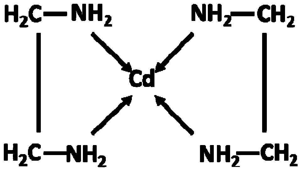
[0042] (1) CdTe nanocrystals (S.Sun, H.M.Liu, Y.P.Gao, D.H.Qin, J.Materials.Chemistry., 2012,517,6853-6856.) were prepared by solvothermal method, and then dissolved in an organic solvent (pyridine and n-propanol mixed solution) to obtain a black solution, that is, a nanocrystal solution, and deposit the nanocrystal solution on the window layer (consisting of successively stacked ITO glass substrates, ZnO layers, and CdSe layers) by spin coating, wherein the ITO / In the ZnO / CdSe device, the thickness of the ITO glass substrate is 150nm, the thickness of the ZnO layer is 40nm, and the thickness of the CdSe layer is 60nm), and then immersed in a saturated cadmium chloride methanol solution, and treated at a high temperature of 380°C to obtain nanocrystals Single-layer, and then solution processing by layer-by-layer stacking can effectively reduce interface defects and internal stress, uniform and dense photoactive layer (CdTe nanocrystalline film), CdTe nanocrystalline film prepa...
Embodiment 2
[0048] (1) CdTe nanocrystals (S.Sun, H.M.Liu, Y.P.Gao, D.H.Qin, J.Materials.Chemistry., 2012,517,6853-6856.) were prepared by solvothermal method, and then dissolved in an organic solvent (pyridine and n-propanol) to obtain a black solution, that is, a nanocrystal solution, and deposit the nanocrystal solution on the window layer (consisting of sequentially stacked ITO glass substrates, ZnO layers, and CdSe layers) by spin coating, wherein the ITO / ZnO / CdSe device, the thickness of the ITO glass substrate is 150nm, the thickness of the ZnO layer is 40nm, the thickness of the CdSe layer is 60nm), and then immersed in saturated CdCl 2 Methanol solution treatment, high temperature treatment at 380°C to obtain nanocrystalline single layer, and then layer by layer solution processing to obtain a uniform and dense photoactive layer (CdTe nanocrystalline thin film), which can effectively reduce interface defects and internal stress, CdTe nanocrystalline film preparation can refer to ...
Embodiment 3
[0054] (1) CdTe nanocrystals (S.Sun, H.M.Liu, Y.P.Gao, D.H.Qin, J.Materials.Chemistry., 2012,517,6853-6856.) were prepared by solvothermal method, and then dissolved in an organic solvent (pyridine and n-propanol) to obtain a black solution, that is, a nanocrystal solution, and deposit the nanocrystal solution on the window layer (consisting of sequentially stacked ITO glass substrates, ZnO layers, and CdSe layers) by spin coating, wherein the ITO / ZnO / CdSe device, the thickness of the ITO glass substrate is 150nm, the thickness of the ZnO layer is 40nm, and the thickness of the CdSe layer is 60nm), and then immersed in a saturated methanol solution of cadmium chloride, and treated at a high temperature of 380 ° C to obtain Nanocrystalline monolayer, and then layer-by-layer solution processing can effectively reduce interface defects and internal stress, uniform and dense CdTe nanocrystalline film, CdTe nanocrystalline film preparation can refer to the literature (Miaozi L, Xin...
PUM
| Property | Measurement | Unit |
|---|---|---|
| Thickness | aaaaa | aaaaa |
| Concentration | aaaaa | aaaaa |
| Thickness | aaaaa | aaaaa |
Abstract
Description
Claims
Application Information
 - R&D Engineer
- R&D Manager
- IP Professional
- Industry Leading Data Capabilities
- Powerful AI technology
- Patent DNA Extraction
Browse by: Latest US Patents, China's latest patents, Technical Efficacy Thesaurus, Application Domain, Technology Topic, Popular Technical Reports.
© 2024 PatSnap. All rights reserved.Legal|Privacy policy|Modern Slavery Act Transparency Statement|Sitemap|About US| Contact US: help@patsnap.com