Low-on-resistance trench silicon carbide power device and manufacturing method thereof

A technology of low on-resistance and power devices, applied in the field of new trench silicon carbide power devices and their manufacturing, can solve the problem that the channel electron mobility of silicon carbide power devices is reduced, the device off current is increased, and the process is difficult. and other problems, to achieve the effect of fast electron saturation drift speed, improved current transmission capacity, and reduced on-resistance

Active Publication Date: 2019-08-27
SOUTHEAST UNIV
View PDF6 Cites 8 Cited by
  • Summary
  • Abstract
  • Description
  • Claims
  • Application Information

AI Technical Summary

Problems solved by technology

Although the manufacturing process of silicon carbide devices has gradually matured and some products have been commercialized, the channel electron mobility of silicon carbide power devices is greatly reduced due to the existence of a large number of interface states between the silicon carbide semiconductor and the silicon dioxide oxide layer. Reduced, can not play the full performance of silicon carbide material
Graphene is a two-dimensional electronic material with high electron mobility, which can be directly grown on silicon carbide substrates. Applying graphene to the field of silicon carbide power devices can greatly reduce the on-resistance of silicon carbide power devices, but It will increase the shutdown current of the device and affect the shutdown characteristics of the device
Moreover, using the traditional silicon carbide epitaxial growth method to manufacture graphene layers requires a high temperature environment above 1400 ° C, which is incompatible with the manufacturing process of silicon carbide power devices, and the chemical vapor deposition method involves wet transfer of graphene layers. The process is difficult and easy to introduce pollution

Method used


Image

  • Low-on-resistance trench silicon carbide power device and manufacturing method thereof
  • Low-on-resistance trench silicon carbide power device and manufacturing method thereof
  • Low-on-resistance trench silicon carbide power device and manufacturing method thereof

Examples


Embodiment 1

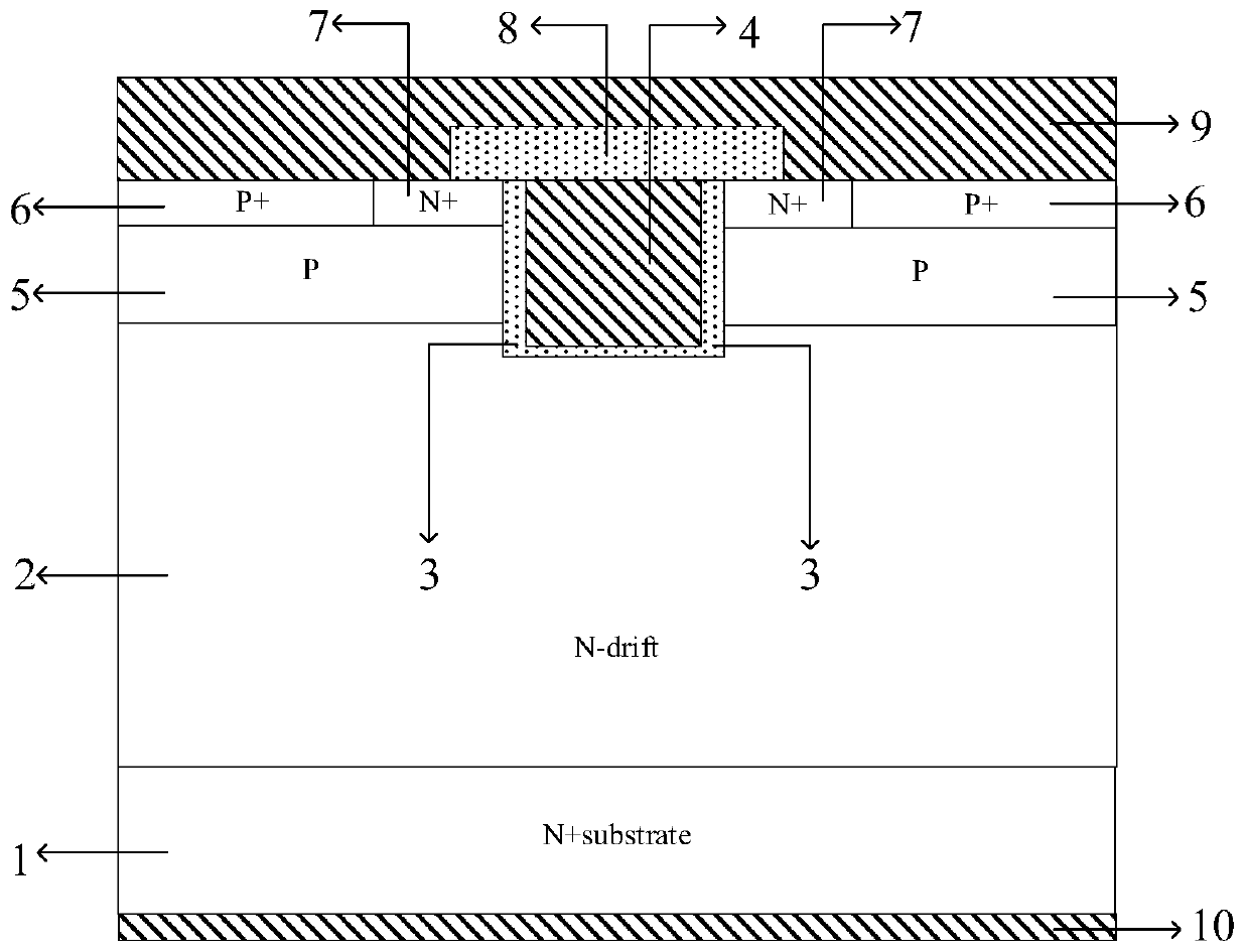
[0032] A trenched SiC power device with low on-resistance, such as figure 2 As shown, it includes: an N-type substrate 1, a drain metal 10 is arranged on one surface of the N-type substrate 1, an N-type epitaxial layer 2 is arranged on the other surface of the N-type substrate 1, and an N-type epitaxial layer 2 is arranged on the N-type substrate 1. The epitaxial layer 2 is provided with a P-type body region 5, an N-type source region 7 and a P-type body contact region 6 are arranged on the P-type body region 5, and the P-type body contact region 6 is located outside the N-type source region 7. The N-type source region 7 and the P-type body contact region 6 are connected with a source metal 9, and a trench is provided in the N-type source region 7, and the trench starts from the surface, depth and N-type epitaxial layer of the N-type source region 7 2, a gate oxide layer 3 is provided on the inner wall and bottom of the trench, polysilicon is filled in the gate oxide layer 3 ...

Embodiment 2

[0034] A method for manufacturing a trench silicon carbide power device with low on-resistance,

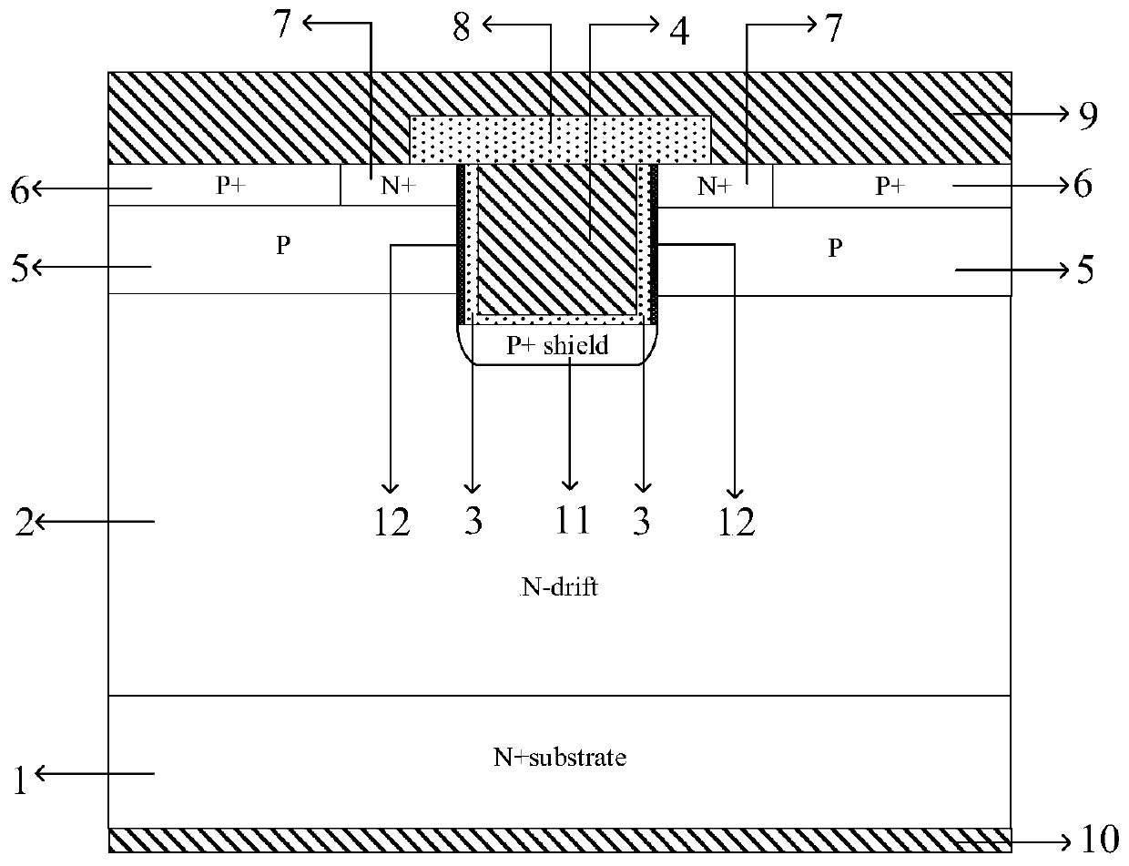
[0035] Step 1 as Figure 6 As shown, take an N-type substrate 1, attach silicon carbide on the other surface of the N-type substrate 1 to form an N-type epitaxial layer 2, and use an etching process to form a groove on the surface of the N-type epitaxial layer 2 ,

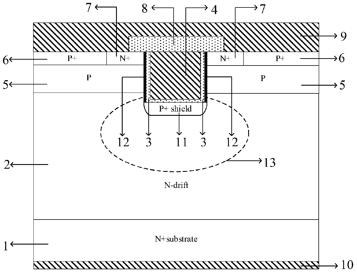
[0036] Step 2 as Figure 7 As shown, using the ion implantation process, a concentration of 10 is formed at the bottom of the trench -4 -10 -6 cm -3 The P-type shielding layer 11,

[0037] Step 3 uses a sputtering process and an etching process to form a layer of metal capable of dissolving carbon on the sidewall of the trench,

[0038]Step 4 Use a high-energy electron beam to bombard the side wall of the trench to break the silicon-carbon bond on the surface of silicon carbide, and generate a local high temperature of 500°C-1200°C in the metal layer that can dissolve carbon, and the carbon generated by the break...


PUM

PropertyMeasurementUnit
thicknessaaaaaaaaaa
angle of incidenceaaaaaaaaaa
thicknessaaaaaaaaaa

Abstract

The invention discloses a low-on-resistance trench silicon carbide power device and a manufacturing method thereof. The cellular structure comprises an N-type substrate, an N-type epitaxial layer anda trench; a graphene layer is arranged on the side wall of the trench; a gate oxide layer and a polycrystalline silicon gate are arranged in the trench; a passivation layer is arranged above the polycrystalline silicon gate; a P-type body region, an N-type source region and a P-type body contact region are arranged on the two sides of the trench; a P-type shielding layer is arranged below the graphene layer; source metal is arranged on the upper surface of the source region; and drain metal is arranged on the lower surface of the substrate. According to the power device, an electron beam method is used, metal and a carbon source gas are used for assisting, and the graphene layer grows on the side wall of the trench. The power device is characterized in that the graphene layer on the side wall of the trench reduces the on resistance. The shielding layer below the graphene layer shields the current flowing through the graphene layer when the device is in an off state, and the turn-off characteristic of the device is improved. The growth of the graphene layer is assisted by metal nickel and the carbon source gas, so that the uniformity, the thickness and the growth rate of the graphene layer are improved.

Description

technical field [0001] The invention belongs to the technical field of structure design and manufacture of power semiconductor devices, and at the same time relates to a manufacturing technology of two-dimensional materials on a wide bandgap semiconductor substrate, specifically a new type of grooved silicon carbide with low on-resistance characteristics Power devices and methods of manufacturing the same. Background technique [0002] Silicon carbide has excellent electrical and thermal properties and is considered to be the most promising third-generation semiconductor material to replace silicon in the field of power electronics. Although the manufacturing process of silicon carbide devices has gradually matured and some products have been commercialized, the channel electron mobility of silicon carbide power devices is greatly reduced due to the existence of a large number of interface states between the silicon carbide semiconductor and the silicon dioxide oxide layer. ...

Claims


Application Information

Patent Timeline
Patent Type & Authority Applications(China)
IPC IPC(8): H01L29/78H01L29/16H01L29/10H01L21/263H01L21/336H01L29/06
CPCH01L29/7813H01L29/66734H01L29/1054H01L29/1606H01L29/1608H01L21/2636H01L29/0615
Inventor 魏家行付浩赵航波刘斯扬孙伟锋陆生礼时龙兴
Owner SOUTHEAST UNIV
Why Eureka
Try Eureka