Multi-channel trench insulated gate bipolar transistor and manufacturing method thereof

A technology of bipolar transistors and insulated gates, applied in semiconductor/solid-state device manufacturing, semiconductor devices, electrical components, etc., can solve problems such as gate dielectric reliability, reduce conductance modulation effects in drift regions, and device breakdown.

Inactive Publication Date: 2021-04-23
SOUTHEAST UNIV
View PDF6 Cites 3 Cited by
  • Summary
  • Abstract
  • Description
  • Claims
  • Application Information

AI Technical Summary

Problems solved by technology

However, the trench IGBT mainly faces two problems: first, the introduction of the trench gate structure brings reliability problems of the gate dielectric, which will cause early breakdown of the d

Method used


Image

  • Multi-channel trench insulated gate bipolar transistor and manufacturing method thereof
  • Multi-channel trench insulated gate bipolar transistor and manufacturing method thereof
  • Multi-channel trench insulated gate bipolar transistor and manufacturing method thereof

Examples


Embodiment 1

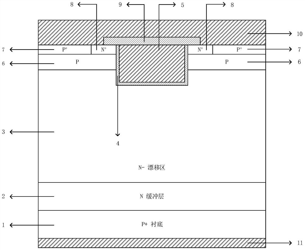
[0039] A multi-channel trench insulated gate bipolar transistor, comprising a P-type substrate 1, a collector metal 11 is arranged on one surface of the P-type substrate 1, and a collector metal 11 is arranged on the other surface of the P-type substrate 1. There is an N-type buffer layer 2, an N-type drift region 3 is arranged on the N-type buffer layer 2, a first P-type base region 6 is arranged on the N-type drift region 3, and a first P-type base region 6 is arranged on the first P-type base region 6. The first P-type contact region 7 and the first N-type emitter region 8, and the first P-type contact region 7 is located outside the first N-type emitter region 8, and a ditch is opened on the first N-type emitter region 8 and the trench is deep into the N-type drift region 3, a gate oxide layer 4 is provided on the inner wall and bottom of the trench, and a polysilicon gate 5 is provided in the gate oxide layer 4, covering the trench There is a passivation layer 9, and a fi...

Embodiment 2

[0048] A method for manufacturing a multi-channel trench insulated gate bipolar transistor,

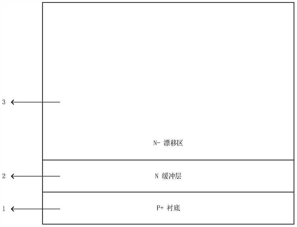
[0049] Step 1: Take a P-type substrate layer 1, grow and form an N-type buffer layer 2 and an N-type drift region 3 on the P-type substrate layer 1;

[0050] Step 2: using an etching process to open a trench on the N-type drift region 3;

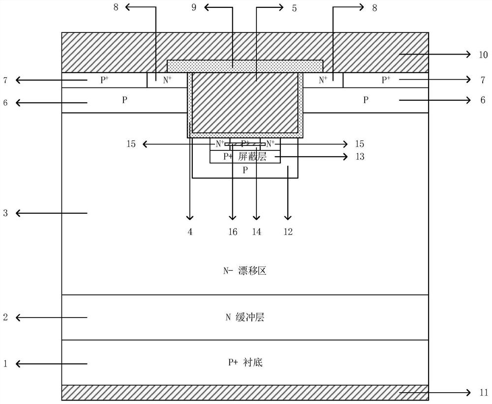
[0051] Step 3: performing ion implantation of P-type impurities at the bottom of the trench to form a second P-type base region 12;

[0052] Step 4: performing ion implantation of P-type impurities to form the P-type shielding layer 13 below the trench;

[0053] Step 5: perform ion implantation of heavily doped P-type impurities to form a second P-type contact region 14 below the trench; then perform ion implantation of N-type impurities to form a second N-type emitter region 15 below the trench;

[0054] Step 6: using a chemical vapor deposition process, forming a gate oxide layer 4 on the sidewall and bottom of the trench and filling the trench ...


PUM

PropertyMeasurementUnit
Thicknessaaaaaaaaaa
Widthaaaaaaaaaa
Thicknessaaaaaaaaaa

Abstract

The invention provides a multi-channel trench insulated gate bipolar transistor and a manufacturing method thereof. The multi-channel trench insulated gate bipolar transistor comprises a P-type substrate, an N-type buffer layer, an N-type drift region, a first P-type base region, a first P-type contact region, and a first N-type emitter region. A second P-type base region, a second P-type contact region, a second N-type emitter region and a P-type shielding layer are arranged below a trench. A gate oxide layer is arranged on the inner wall and the bottom of the trench, and a polysilicon gate is arranged in the gate oxide layer. The trench is covered with a passivation layer, first emitter metal and second emitter metal are formed on the upper surface, and collector metal is formed on the lower surface of the P-type substrate. Before the trench is formed, ion implantation of P-type impurities and N-type impurities is performed below the trench for multiple times, and the emitter implantation effect is improved, so that a relatively strong drift region conductivity modulation effect is generated, the resistivity of the drift region is remarkably reduced, and the on-resistance of the device is greatly reduced; and meanwhile, a conductive channel is added, so that the channel resistance is reduced.

Description

technical field [0001] The invention belongs to the technical field of power semiconductor device structure design and manufacture, and mainly relates to a multi-channel trench device structure, and also relates to its manufacturing technology on a wide-bandgap semiconductor substrate, specifically a multi-channel trench device structure. Trench insulated gate bipolar transistor and method of manufacturing the same. Background technique [0002] One problem with SiC devices is that due to its high interface trap density, the channel carrier mobility is significantly lower than the bulk carrier mobility, and the channel on-resistance occupies a considerable part of the total on-resistance of the device. ratio, making it difficult to obtain the expected low on-resistance. Insulated gate bipolar transistor (Insulated gate bipolartransistor, IGBT) is a composite device combining MOS voltage control and bipolar transistor. It has the advantages of high input impedance and easy d...

Claims


Application Information

Patent Timeline
IPC IPC(8): H01L29/739H01L29/423H01L29/167H01L21/331
CPCH01L29/66348H01L29/7397H01L29/4236H01L29/167
Inventor 刘斯扬严晓雯付浩隗兆祥周华魏家行孙伟锋时龙兴
Owner SOUTHEAST UNIV
Why Eureka
Try Eureka