Bragg reflecting mirror based on BN(Al) film, and preparation method
A technology of Bragg reflectors and thin films, applied in mirrors, sputtering coatings, ion implantation coatings, etc., can solve problems such as difficult effective control of different center wavelengths, high requirements for preparation technology, small difference in refractive index, etc., and achieve process Simple, highly reflective, low-cost effects
- Summary
- Abstract
- Description
- Claims
- Application Information
AI Technical Summary
Problems solved by technology
Method used
Image
Examples
Embodiment approach
[0040] In order to better understand the solutions of the present invention, the present invention will be further described in detail below in conjunction with specific embodiments.
[0041] Boron nitride (BN) has excellent electrical insulation, excellent chemical stability and excellent dielectric properties, and has been paid more and more attention by scientific researchers. BN is a wide bandgap semiconductor material, which has great application potential in semiconductor light-emitting devices. On the other hand, magnetron sputtering technology, one of the most important coating industrial methods at present, can prepare almost all metals, alloys and ceramic materials. Dual power sputtering method is adopted, one power source sputters the hexagonal BN target, and the other power source sputters the metal Al target. By adjusting the sputtering power, BAlN with precise and constant ratio can be deposited, and at the same time, the sputtering coating can be accurately cont...
Embodiment 1
[0044] Based on a silicon substrate, a thin-film periodic structure in a Bragg mirror is fabricated as follows:
[0045] (1) Silicon substrate cleaning: heat the 311 (hydrogen peroxide and sulfuric acid 3:1 mixture) solution and soak at 180°C for 15-20 minutes, then immerse the silicon substrate in absolute ethanol for ultrasonic cleaning for 15 minutes, and then rinse with deionized water three times Finally, blow dry with nitrogen to remove impurities attached to the surface of the silicon substrate.
[0046] (2) Sputtering: Send the clean silicon substrate into the sputtering chamber to heat up, and the temperature rise rate does not exceed 10°C / min. Set the preset temperature to 600°C, and the holding time is not less than the sputtering time (in this case, the holding time is set to 6h) to ensure the stability of the temperature of the chamber and the substrate. A dual power supply magnetron sputtering method is adopted, with high-purity hexagonal BN target material (99....
Embodiment 2
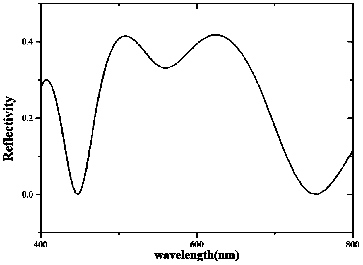
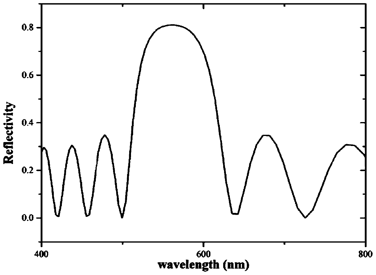
[0050] see figure 2 , based on the preparation process parameters of a thin film periodic structure BN / BAlN thin film, the thickness is 71nm / 83nm respectively, the thickness of a thin film periodic structure is 154nm, the thickness of 1 / 4 wavelength is 140nm, and the number of preparation cycles is 5, the wavelength range can be obtained in 450nm In the range of -650nm, the reflectivity reaches more than 33%.
PUM
| Property | Measurement | Unit |
|---|---|---|
| thickness | aaaaa | aaaaa |
| thickness | aaaaa | aaaaa |
| thickness | aaaaa | aaaaa |
Abstract
Description
Claims
Application Information


