Semiconductor laser and laser resonant cavity and optical confinement structure thereof
A laser resonator and confinement structure technology, applied in the field of lasers, can solve problems such as adverse device performance and impact, and achieve the effect of improving yield
- Summary
- Abstract
- Description
- Claims
- Application Information
AI Technical Summary
Problems solved by technology
Method used
Image
Examples
Embodiment 1
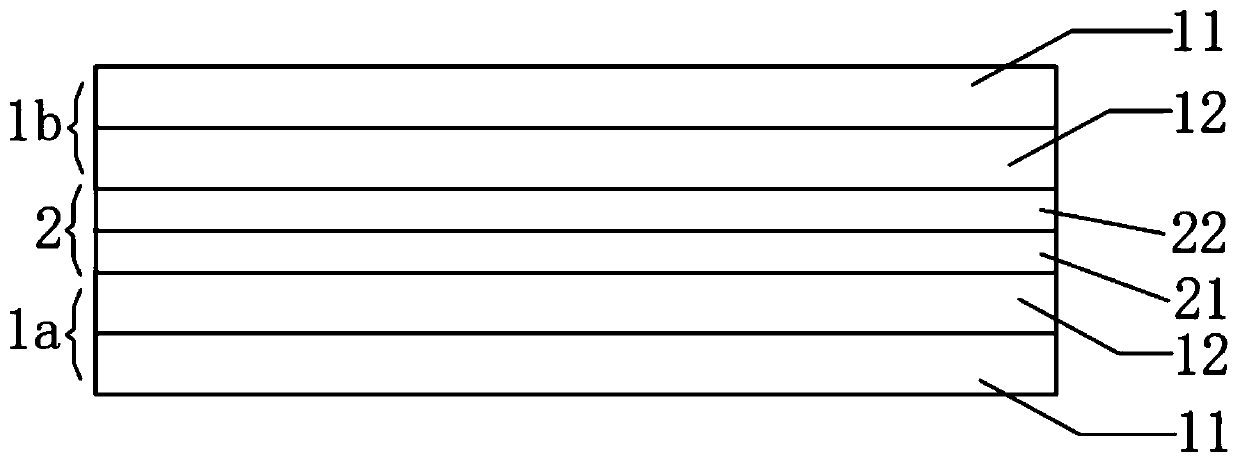
[0025] Such as figure 1 As shown, this embodiment provides an optical confinement structure 1 for forming a laser resonator. The optical confinement structure 1 of this embodiment includes a waveguide layer 12 and a cladding layer 11 disposed on the surface of the waveguide layer 12 . The refractive index of the cladding layer 11 is smaller than that of the waveguide layer 12 . The cladding layer 11 is used to reflect light entering the cladding layer 11 from the waveguide layer 12 .
[0026] Specifically, in this embodiment, the cladding layer 11 is aluminum indium gallium nitride (Al x In y Ga 1-x-y N) Quaternary alloys. Aluminum Indium Gallium Nitride (AlInGaN x In y Ga 1-x-y The bandgap and forbidden band width of N) are jointly determined by the components of aluminum and gallium, and the lattice parameter and forbidden band width (refractive index) of the cladding layer 11 can be adjusted simultaneously. In this way, while reducing the refractive index of the cl...
Embodiment 2
[0033] This embodiment provides a laser resonant cavity. Such as figure 2 As shown, the laser resonator includes a first optical confinement structure 1a and a second optical confinement structure 1b. It should be noted that both the first optical confinement structure 1 a and the second optical confinement structure 1 b are the optical confinement structures 1 provided in Embodiment 1. Wherein, the waveguide layer 12 of the first optical confinement structure 1 a and the waveguide layer 12 of the second optical confinement structure 1 b are arranged facing each other.
[0034] Specifically, the absolute value of the refractive index difference between the waveguide layer 12 and the cladding layer 11 of the first optical confinement structure 1a is larger than that between the waveguide layer 12 and the cladding layer 11 of the second optical confinement structure 1b. The absolute value of the refractive index difference between the cladding layers 11 . It should be noted ...
Embodiment 3
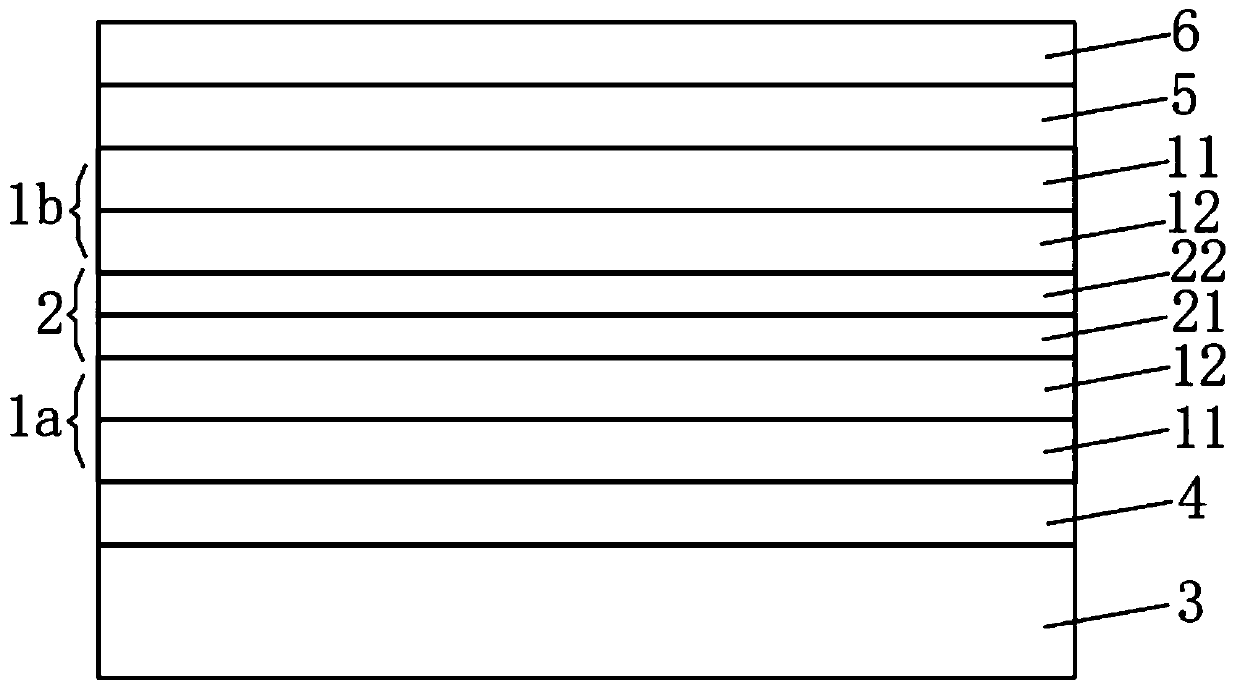
[0037] This embodiment provides a semiconductor laser. Such as image 3 as shown, image 3 A laser unit of the laser in this embodiment is shown, and the laser unit includes the substrate 3 and the laser cavity provided in the second embodiment. The cladding layer 11 of the first optical confinement structure 1 a of the laser resonator is disposed on the substrate 3 . A quantum well active layer 2 is provided between the waveguide layer 12 of the first optical confinement structure 1a and the waveguide layer 12 of the second optical confinement structure 1b.
[0038] Specifically, combined with figure 2 As is known, the quantum well active layer 2 includes a stacked quantum well single layer 21 and a quantum well barrier single layer 22, wherein the quantum well single layer 21 faces the first optical confinement structure 1a, and the quantum well The single well barrier layer 22 faces the second optical confinement structure 1b.
[0039] Preferably, an N-type GaN layer ...
PUM
| Property | Measurement | Unit |
|---|---|---|
| Growth temperature | aaaaa | aaaaa |
| Growth pressure | aaaaa | aaaaa |
Abstract
Description
Claims
Application Information


