
Near-zero dielectric constant controllable substrate and preparation method thereof

A near-zero dielectric constant technology, applied in the field of near-zero dielectric constant controllable substrates and its preparation, can solve the problems of complex operation and long experimental cycle, and achieve broad application prospects, short process cycle, and short time-consuming Effect

Inactive Publication Date: 2019-11-15
UNIV OF SHANGHAI FOR SCI & TECH
View PDF12 Cites 1 Cited by
  • Summary
  • Abstract
  • Description
  • Claims
  • Application Information

AI Technical Summary

Problems solved by technology

In recent years, the regulation of the ENZ mode is mostly achieved by doping substances and changing its growth conditions. The experiment period is long and the operation is complicated.

Method used


Image

  • Near-zero dielectric constant controllable substrate and preparation method thereof
  • Near-zero dielectric constant controllable substrate and preparation method thereof
  • Near-zero dielectric constant controllable substrate and preparation method thereof

Examples


Embodiment 1

[0028] This embodiment describes the preparation method of a substrate with a controllable near-zero dielectric constant.

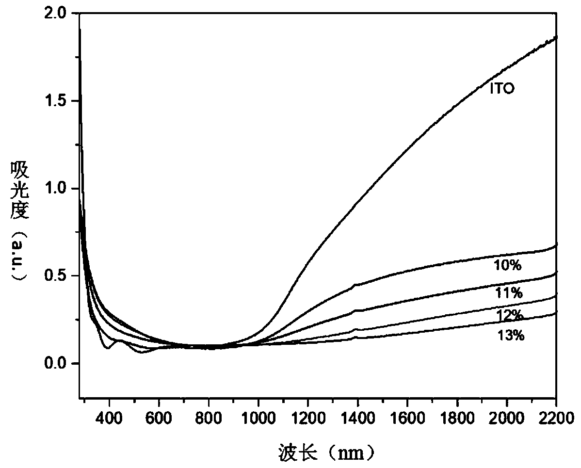
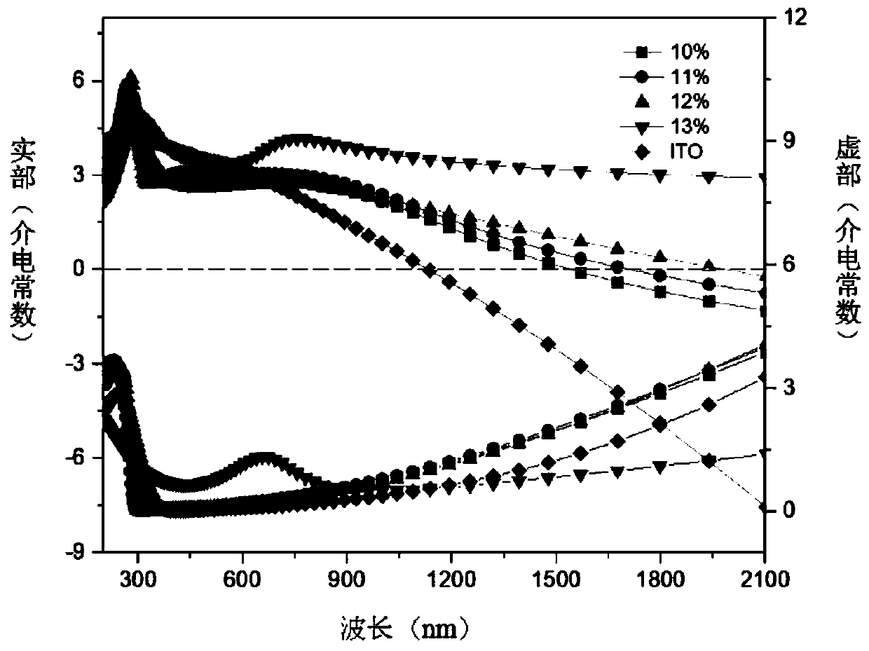
[0029] Step 1. Place the clean substrate in the electron beam vacuum evaporation equipment, and deposit a film material with near-zero dielectric constant on the substrate by electron beam evaporation to obtain a transparent and conductive film.

[0030] In this embodiment, indium tin oxide (ITO) with a purity of 99.99% is selected as the film material, and 90wt.% (indium oxide) In 2 o 3 and 10wt.% (tin oxide) SnO 2 composition. A quartz substrate was chosen as the substrate. Keep the vacuum in the electron beam vacuum evaporation equipment below 9.0×10 -4 Pa, deposit ITO on the surface of the quartz substrate to obtain a 300nm thick transparent and conductive ITO film.

[0031] Step 2: In the atmospheric environment, a pulsed laser is used to irradiate the surface of the film with certain laser parameters, so that the film is modified to obtain a su...

Embodiment 2

[0034] In this embodiment, except that the laser power used by the 1064 nanosecond pulsed laser is different when irradiating the ITO thin film, the remaining parts are the same as in Embodiment 1, so details are not repeated here. In this embodiment, the laser power is 10% of the total laser power, that is, 2.2w.

Embodiment 3

[0036] In this embodiment, except that the laser power used by the 1064 nanosecond pulsed laser is different when irradiating the ITO thin film, the remaining parts are the same as in Embodiment 1, so details are not repeated here. In this embodiment, the laser power is 12% of the total laser power, that is, 2.4w.


PUM


Abstract

The invention provides a near-zero dielectric constant controllable substrate and a preparation method thereof. The method comprises the following steps of placing a clean substrate in electron beam vacuum evaporation equipment, and depositing a film material with a near-zero dielectric constant characteristic on a substrate by adopting an electron beam evaporation method to obtain a transparent conductive film; in an atmospheric environment, irradiating the surface of the film with a certain laser parameter by adopting a pulse laser, and modifying the film to obtain the near-zero dielectric constant controllable substrate. The preparation method of the near-zero dielectric constant controllable substrate provided by the invention is low in preparation cost and short in process period; theregulation of a large-waveband range of a dielectric constant real part near-zero point can be conveniently obtained by adjusting the laser parameter; the prepared near-zero dielectric constant controllable substrate has good sensitivity, and the near-zero dielectric constant controllable substrate and the preparation method thereof have a wide application prospect in the fields of photonic devices, optical interconnection, photonic signal processing and CMOS compatible nonlinear optics, and the like.

Description

technical field [0001] The invention belongs to the technical field of film surface modification, and in particular relates to a controllable near-zero dielectric constant substrate and a preparation method thereof. Background technique [0002] Near-zero dielectric constant (ENZ, Epsilon near zero) metamaterials refer to a class of metamaterials whose relative permittivity approaches zero infinitely. When the relative permittivity approaches zero, the phase velocity will become very large, the impedance is close to zero for light waves, and the phase change is infinitely small. Therefore, ENZ metamaterials can directional emit electromagnetic waves or shape the phase ahead. In addition, ENZ metamaterials can also modulate the polarization direction of light, and enhance the nonlinearity of light, spontaneous emission rate and photon density of states. [0003] The ENZ mode is a strong local resonance mode, which only exists in sub-wavelength nanomaterials with zero or near...

Claims


Application Information

Patent Timeline
IPC IPC(8): C23C14/30C23C14/08C23C14/06C23C14/58
CPCC23C14/0641C23C14/086C23C14/30C23C14/58
Inventor 洪瑞金颜廷贞张大伟师境奇李正旺陶春先
Owner UNIV OF SHANGHAI FOR SCI & TECH
Learn More